PhaseLink PLL650-04
The PLL650-04 provides selectable spread spectrum modulation and selectable output frequencies for the CLKOUT signal. In order to reduce the number of pins on the chip, the PLL650-04 uses bi-directional pins that serve as inputs upon power-up, and as outputs as soon as the inputs have been latched.| Part No. | PLL650-04 |
|---|---|
| Datasheet | PLL650-04 Download |
| Manufacturer |  PhaseLink |
| Description | Low EMI Clock |
| Buy | Stock & Price |
FEATURES
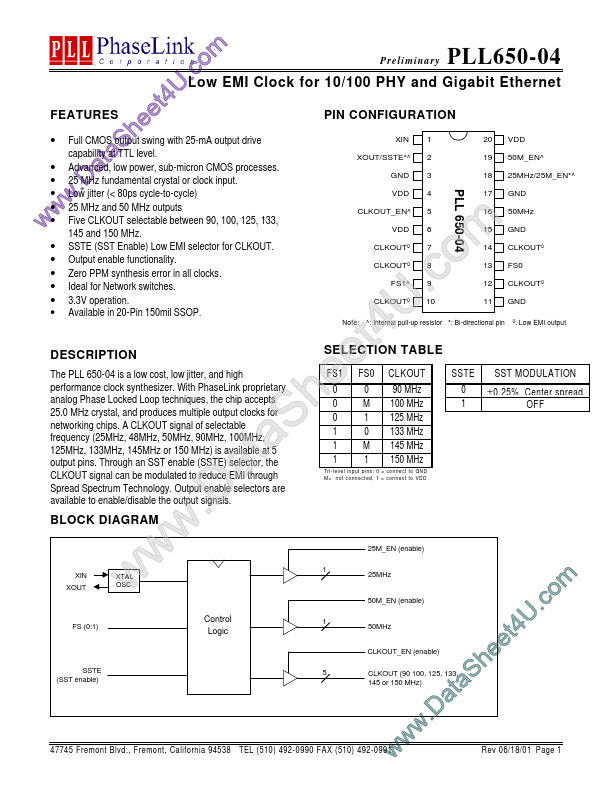
PIN CONFIGURATION e hswing with 25-mA output drive● Full CMOS output S capability at TTL level. a t
● Advanced, low power, sub-micron CMOS processes. a
● 25 MHz .D fundamental crystal or clock input.
● Low jitter (< 80ps cycle-to-cycle) w
● 25 MHz and 50 MHz outputs w CLKOUT selectable between 90, 100, 125, 133, w● Five 145 and 150 MHz. XIN 1 2 3 4 5 6 7 8 9 20 19 18 17 16 15 14 13 12 VDD XOUT/SSTE*^ GND 50M_EN^ 25MHz/25M_EN*^ GND PLL 650-04 VDD
●
●
●
●
●
● SSTE (SST Enable) Low EMI selector for CLKOUT. Output enable functionality. Zero PPM synthesis error in all clocks. Ideal for Network switches. 3.3V operation. Available in 20-Pin 150mil SSOP.
DESCRIPTION
The PLL 650-04 is a low cost, low jitter, and high performance clock synthesizer. With PhaseLink proprietary analog Phase Locked Loop techniques, the chip accepts 25.0 MHz crystal, and produces multiple output clocks for networking chips. A CLKOUT signal of selectable frequency (25MHz, 48MHz, 50MHz, 90MHz, 100MHz, 125MHz, 133MHz, 145MHz or 150 MHz) is available at 5 output pins.