PhaseLink PLL650-08
The order number for this device is a combination of the following: Device number, Package type and Operating temperature range PLL650-08 S C PART NUMBER TEMPERATURATURE C=COMMERCIAL M=MILITARY I=INDUSTRAL PACKAGE TYPE S=SOIC PhaseLink Corporation, reserves the right to make changes in its products or specifications, or both at any time without notice. The information furnished by Phaselink is believed to be accurate and reliable.| Part No. | PLL650-08 |
|---|---|
| Datasheet | PLL650-08 Download |
| Manufacturer |  PhaseLink |
| Description | Network LAN Clock Source |
| Buy | Stock & Price |
FEATURES
●●
●
●
●
●
●
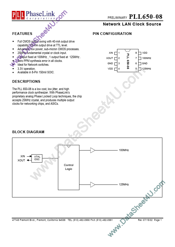
● w w Full CMOS output swing with 40-mA output drive capability. 25-mA output drive at TTL level. Advanced, low power, sub-micron CMOS processes. 25MHz fundamental crystal or clock input. 1 output fixed at 100MHz , 1 output fixed at 125MHz . Zero PPM synthesis error in all clocks. Ideal for Network switches. 3.3V operation. Available in 8-Pin 150mil SOIC. at .D w h S a t e e 4U m o .c PRELIMINARY PLL650-08 Network LAN Clock Source PIN CONFIGURATION XIN XOUT GND VDD 1 2 3 4 8 7 6 5 VDD 100MHz GND 125MHz PLL 650-08 DESCRIPTIONS The PLL 650-08 is a low cost, low jitter, and high performance clock synthesizer. With PhaseLink’s proprietary analog Phase Locked Loop techniques, the chip accepts 25MHz crystal, and produces multiple output clocks for networking chips, and ASICs. BLOCK DIAGRAM XIN XOUT XTAL OSC w w w t a .D Control Logic S a e h U 4 t e .c m o 100MHz 125MHz 47745 Fremont Blvd., Fremont, California 94538 TEL (510) 492-0990 FAX (510) 492-0991 w w w .D a S a...

