74F323
74F323 is 8-bit universal shift/storage register manufactured by Philips Semiconductors.
FEATURES
- mon parallel I/O for reduced pin count
- Additional serial inputs and outputs for expansion
- Four operating modes: Shift left, shift right, load, and store
- 3-State outputs for bus-oriented applications
DESCRIPTION
The 74F323 is an 8-bit universal shift/storage register with 3-State outputs. Its function is similar to the 74F299 with the exception of synchronous Reset. Parallel load inputs and flip-flop outputs are multiplexed to minimize pin counts. Separate serial inputs and outputs are provided for flip-flops Q0 and Q7 to allow easy serial cascading. Four modes of operation are possible: Hold (store), shift left, shift right, and parallel load. The 74F323 contains eight edge-triggered D-type flip-flops and the interstage logic necessary to perform synchronous reset, shift left, shift right, parallel load, and hold operations. The type of operation is determined by S0 and S1, as shown in the Function Table. All flip-flop outputs are brought out through 3-State buffers to separate I/O pins that also serve as data inputs in the parallel load mode. Q0 and Q7 are also brought out on other pins for expansion in serial shifting of longer words. A Low signal on SR overrides the Select and inputs and allows the flip-flops to be reset by the next rising edge of clock. All other state changes are initiated by the rising edge of the clock. Inputs can change when the clock is in either state provided only that the remended setup and hold times, relative to the rising edge of clock are observed. A High signal on either OE0 or OE1 disables the 3-State buffers and puts the I/O pins in the high impedance state. In this condition the shift, hold, load and reset operations can still occur. The 3-State buffers are also disabled by High signals on both S0 and S1 in preparation for a parallel load operation.
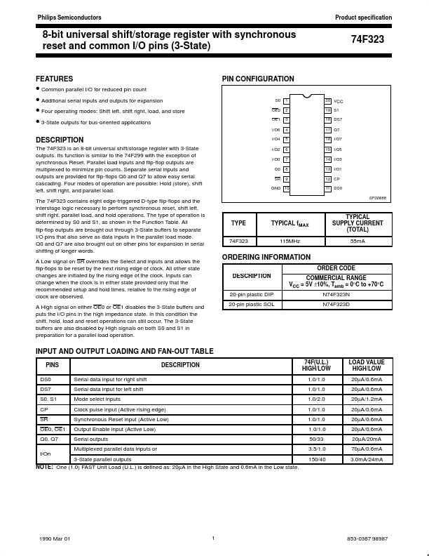
PIN CONFIGURATION
S0 OE0 OE1 I/O6 I/O4 I/O2 I/O0 Q0 SR 1 2 3 4 5 6 7 8 9 20 VCC 19 S1 18 DS7 17 Q7 16 I/O7 15 I/O5 14 I/O3 13 I/O1 12 CP 11 DS0
GND...