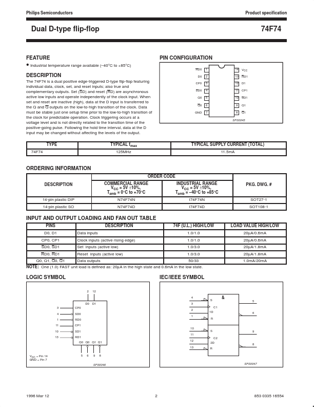
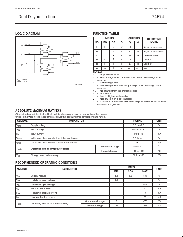
DESCRIPTION
Set (SD) and reset (RD) are asynchronous active low inputs and operate independently of the clock input. Data must be stable just one setup time prior to the low-to-high transition of the clock for predictable operation. Clock triggering occurs at a voltage level and is not directly related to the transition time of the positive-going pulse. Following the hold time interval, data at the D input may be changed without affecting the levels of the output. TYPE 74F74 TYPICAL fmax 125MHz PIN CONFIGURATION RD0 D0 CP0 SD0 Q0 Q0 GND 1 2 3 4 5 6 7 14 13 12 11 10 9 8 VCC RD1 D1 CP1 SD1 Q1 Q1 SF00045 TYPICAL SUPPLY CURRENT (TOTAL) 11.5mA ORDERING INFORMATION ORDER CODE DESCRIPTION
COMMERCIAL RANGE VCC = 5V ±10%, Tamb = 0°C to +70°C N74F74N N74F74D INDUSTRIAL RANGE VCC = 5V ±10%, Tamb = –40°C to +85°C I74F74N I74F74D PKG. DWG. # 14-pin plastic DIP 14-pin plastic SO SOT27-1 SOT108-1 INPUT AND OUTPUT LOADING AND FAN OUT TABLE PINS D0, D1 CP0, CP1 SD0, SD1 RD0, RD1 Data inputs Clock input... Philips