Philips 74LV257
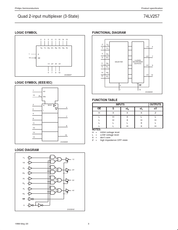
The 74LV257 is a low-voltage Si-gate CMOS device and is pin and function compatible with 74HC/HCT257. The 74LV257 is a quad 2-input multiplexer with 3-state outputs, which select 4 bits of data from two sources and are controlled by a common data select input (S). The data inputs from source 0 (1l0 to 4l0) are selected when input S is LOW and the data inputs from source 1 (1l1 to 4l1) are selected when S in HIGH.| Part No. | 74LV257 |
|---|---|
| Datasheet | 74LV257 Download |
| Manufacturer |  Philips |
| Description | Quad 2-input multiplexer |
| Buy | Stock & Price |

FEATURES
● Optimized for low voltage applications: 1.0 to 3.6 V● Accepts TTL input levels between VCC = 2.7 V and VCC = 3.6 V
● Typical VOLP (output ground bounce) < 0.8 V at VCC = 3.3 V,
● Typical VOHV (output VOH undershoot) > 2 V at VCC = 3.3 V,
● Non-inverting data path
● Output capability: bus driver
● ICC category: MSI Tamb = 25°C Tamb = 25°C
DESCRIPTION
Data appears at the outputs (1Y to 4Y) in true (non-inverting) from the selected inputs. The 74LV257 is the logic implementation of a 4-pole, 2-position switch, where the position of the switch is determined by the logic levels applied to S. The outputs are forced to a high impedance OFF-state when OE is HIGH. The logic equations for the outputs are: 1Y = OE × (1l1 × S + 1l0 × S) 2Y = OE × (2l1 × S + 2l0 × S) 3Y = OE × (3l1 × S + 3l0 × S) 4Y = OE × (4l1 × S + 4l0 × S) QUICK REFERENCE DATA GND = 0 V; Tamb = 25°C; tr = tf ≤ 2.5 ns SYMBOL tPHL/tPLH CI CPD PARAMETER Propagation delay nl0, nl1 to nY S to nY Input capacitance Power dissipation capacitance per gate VI = GND to VCC 1 CONDITIONS CL = 15 pF; VCC = 3.3 V TYPICAL 10 14 3.5 30 UNIT ns pF pF NOTE: 1.