Philips 74LV377
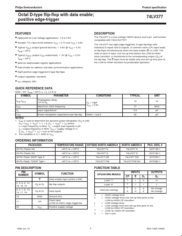
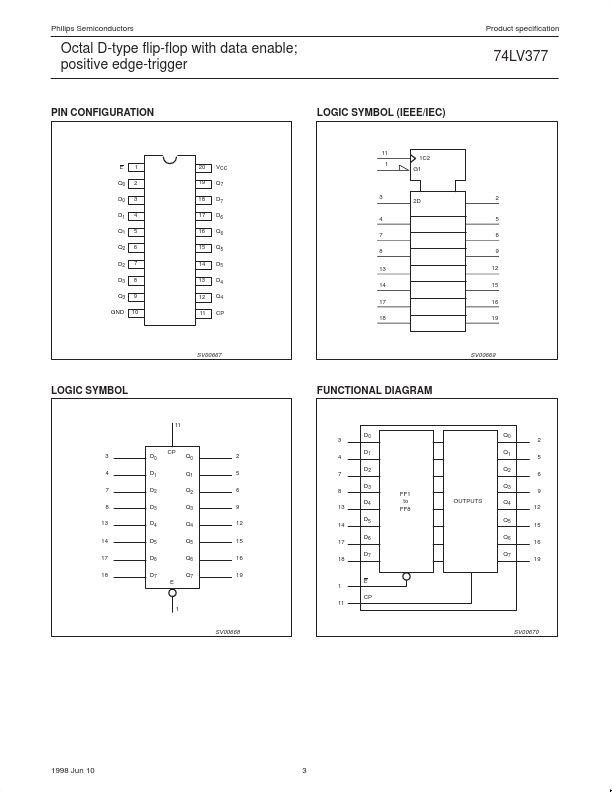
The 74LV377 is a low–voltage CMOS device and is pin and function compatible with 74HC/HCT377. The 74LV377 has eight edge-triggered, D-type flip-flops with individual D inputs and Q outputs. The state of each D input, one set-up time before the LOW-to-HIGH clock transition, is transferred to the corresponding output (Qn) of the flip-flop.| Part No. | 74LV377 |
|---|---|
| Datasheet | 74LV377 Download |
| Manufacturer |  Philips |
| Description | Octal D-type flip-flop |
| Buy | Stock & Price |
FEATURES
● Optimized for Low Voltage applications: 1.0 to 3.6V● Accepts TTL input levels between VCC = 2.7V and VCC = 3.6V
● Typical VOLP (output ground bounce) t 0.8V @ VCC = 3.3V,
● Typical VOHV (output VOH undershoot) u 2V @ VCC = 3.3V,
● Ideal for addressable register applications
● Data enable for address and data synchronization applications
● Eight positive-edge triggered D-type flip-flops
● Output capability: standard
● ICC category: MSI QUICK REFERENCE DATA GND = 0V; Tamb = 25°C; tr = tf v2.5 ns SYMBOL tPHL/tPLH fmax CI CPD PARAMETER Propagation delay CP to Qn Maximum clock frequency Input capacitance Power dissipation capacitance per flip-flop Tamb = 25°C Tamb = 25°C
DESCRIPTION
A common clock (CP) input loads all flip-flops simultaneously when the data enable (E) is LOW. The E input must be stable only one set-up time prior to the LOW-to-HIGH transition for predictable operation. CONDITIONS CL = 15pF VCC = 3.3V 3 3V TYPICAL 13 77 3.5 20 UNIT ns MHz pF pF Notes 1 and 2 NOTES: 1.