DESCRIPTION
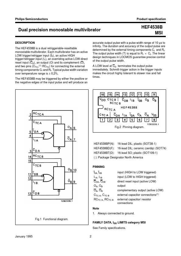
Typical pulse width variation over temperature range is ± 0,2%. The duration and accuracy of the output pulse are determined by the external timing components Ct and Rt. The output pulse width (T) is equal to Rt × Ct. The linear design techniques in LOCMOS guarantee precise control of the output pulse width. A LOW level at CD terminates the output pulse immediately. Schmitt-trigger action in the trigger inputs makes the circuit highly tolerant to slower rise and fall times. Fig.1 Functional diagram. January 1995 Fig.2 Pinning diagram. HEF4538BP(N): 16-lead DIL; plastic (SOT38-1) HEF4538BD(F): 16-lead DIL; ceramic (cerdip) (SOT74) HEF4538BT(D): 16-lead SO; plastic (SOT109-1) ( ): Package Designator North America PINNING I0A, I0B I1A, I1B CDA, CDB OA, OB OA, OB CTC A, CTC B RCTC A, RCTC B input (HIGH to LOW triggered) input (LOW to HIGH triggered) direct reset input (active LOW) output complementary output (active LOW) external capacitor connections(1) external capacitor/ resistor connections Note 1. Philips