DESCRIPTION
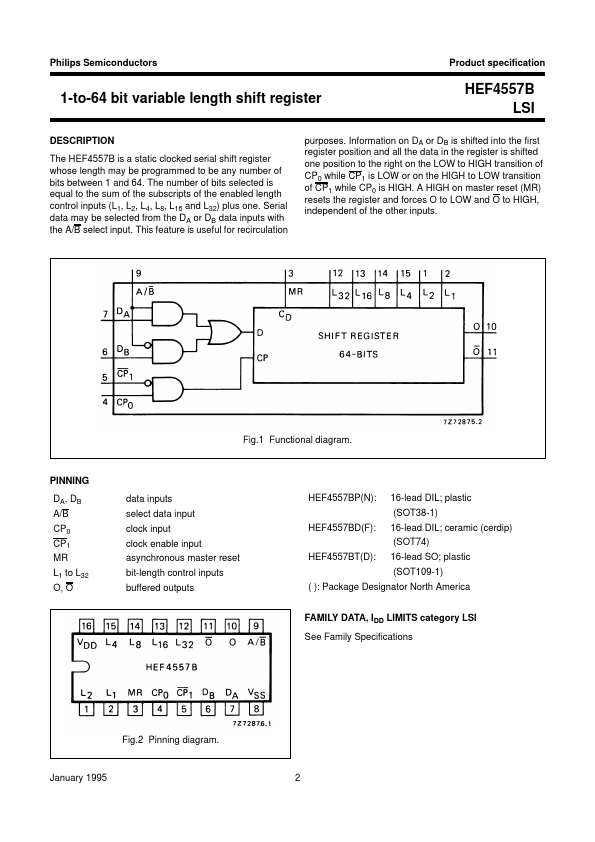
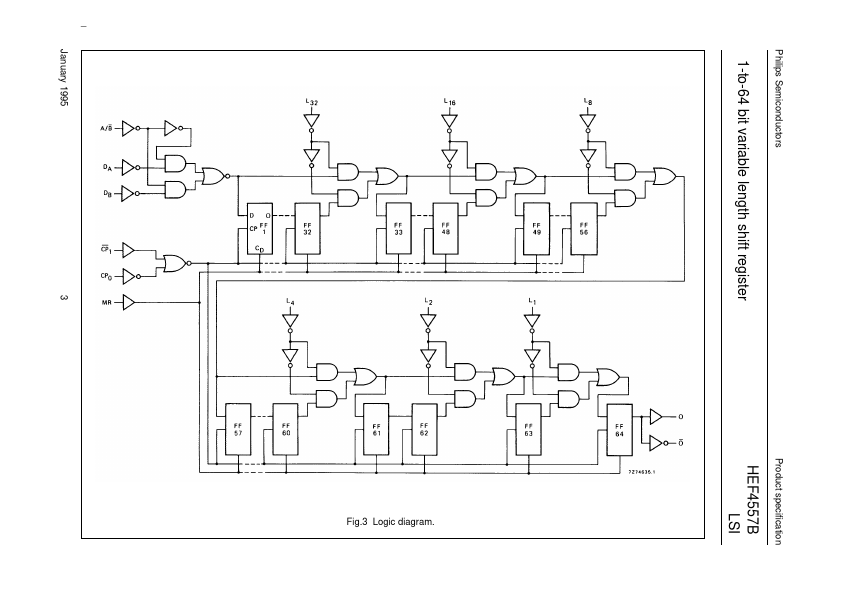
Serial data may be selected from the DA or DB data inputs with the A/B select input. Information on DA or DB is shifted into the first register position and all the data in the register is shifted one position to the right on the LOW to HIGH transition of CP0 while CP1 is LOW or on the HIGH to LOW transition of CP1 while CP0 is HIGH. A HIGH on master reset (MR) resets the register and forces O to LOW and O to HIGH, independent of the other inputs. PINNING DA, DB A/B CP0 CP1 MR L1 to L32 O, O Fig.1 Functional diagram. data inputs select data input clock input clock enable input asynchronous master reset bit-length control inputs buffered outputs HEF4557BP(N): 16-lead DIL; plastic (SOT38-1) HEF4557BD(F): 16-lead DIL; ceramic (cerdip) (SOT74) HEF4557BT(D): 16-lead SO; plastic (SOT109-1) ( ): Package Designator North America FAMILY DATA, IDD LIMITS category LSI See Family Specifications Fig.2 Pinning diagram. January 1995 2 Philips Semiconductors 1-to-64 bit variable length shi... Philips