DESCRIPTION
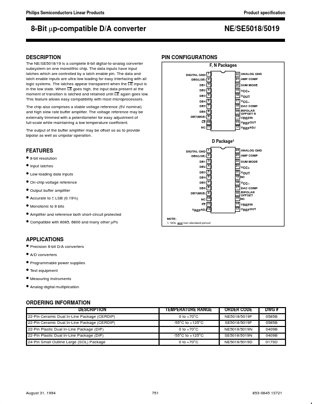
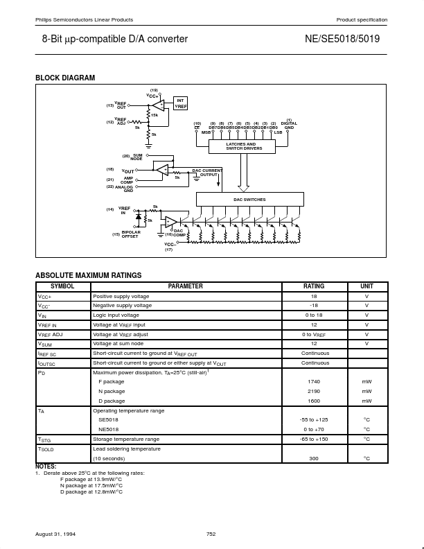
The data and latch enable inputs are ultra-low loading for easy interfacing with all logic systems. The latches appear transparent when the LE input is in the low state. When LE goes high, the input data present at the moment of transition is latched and retained until LE again goes low. This feature allows easy compatibility with most microprocessors. The chip also comprises a stable voltage reference (5V nominal) and high slew rate buffer amplifier. The voltage reference may be externally trimmed with a potentiometer for easy adjustment of full-scale while maintaining a low temperature coefficient. The output of the buffer amplifier may be offset so as to provide bipolar as well as unipolar operation. PIN CONFIGURATIONS F, N Packages DIGITAL GND 1 DB0(LSB) 2 DB1 3 DB2 4 DB3 5 DB4 6 DB5 7 DB6 8 DB7(MSB) 9 LE 10 NC 11 22 ANALOG GND 21 AMP COMP 20 SUM MODE 19 V CC+ 18 V 17 VCC– 16 DAC COMP 15 BIPOLAR OFFSET R 14 V REFIN 13 V OUT OUT REF 12 V REFADJ D Package1 FEATURES
● 8-bi... Philips