DESCRIPTION
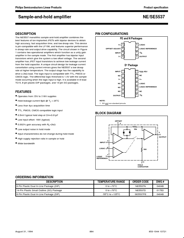
The circuit shown in Figure 1 contains two operational amplifiers which function as a unity gain amplifier in the sample mode. The first amplifier has bipolar input transistors which give the system a low offset voltage. The second amplifier has JFET input transistors to achieve low leakage current from the hold capacitor. A unique circuit design for leakage current cancellation using current mirrors gives the NE5537 a low droop rate at higher temperature. The output stage has the capability to drive a 2kΩ load. The logic input is compatible with TTL, PMOS or CMOS logic. The differential logic threshold is 1.4V with the sample mode occurring when the logic input is high. It is available in 8-lead TO-5, 8-pin plastic DIP packages, and 14-pin SO packages. PIN CONFIGURATIONS FE and N Packages V+ 1 OFFSET ADJUST 2 INPUT 3 V– 4 8 7 6 5 LOGIC LOGIC REFERENCE Ch OUTPUT D1 Package INPUT NC V– NC NC 1 2 3 4 5 6 7 14 V OS ADJ 13 NC 12 V+ 11 LOGIC 10 LOGIC REFERENCE 9 8 NC Ch FEATURES
... Philips