Datasheet Summary
Philips Semiconductors
PC board footprint
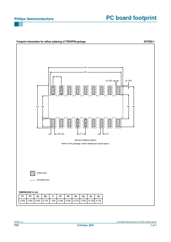
Footprint information for reflow soldering of TSSOP48 package
SOT362-1
Hx Gx P2 (0.125) (0.125)
Hy
Gy
By
Ay
D2 (4x)
P1 Generic footprint pattern
D1
Refer to the package outline drawing for actual layout solder land occupied area
DIMENSIONS in mm P1 0.500 P2 0.560 Ay 8.900 By 6.100 C 1.400 D1 0.280 D2 Gx Gy Hx Hy
0.400 12.270
7.000 14.100 9.150
SOT362-1_fp
© Koninklijke Philips Electronics N.V. 2004. All rights reserved.
8 October 2004
1 of 1...