NE568A
NE568A is 150MHz phase-locked loop manufactured by Philipss.
Philips Semiconductors
Product specification
150MHz phase-locked loop
NE/SA568A
DESCRIPTION
The NE568A is a monolithic phase-locked loop (PLL) which operates from 1Hz to frequencies in excess of 150MHz and Features an extended supply voltage range and a lower temperature coefficient of the VCO center frequency in parison with its predecessor, the NE 568. The NE568A is function and pin-patible with the NE568, requiring only minor changes in peripheral circuitry (see Figure 3). Temperature pensation network is different, no resistor on Pin 12, needs to be grounded and Pin 13 has a 3.9kΩ resistor to ground. Timing cap, C2, is different and for 70MHz operation with temperature pensation network should be 16p F, not 34p F as was used in the NE568. The NE568A has the following improvements: ESD protected; extended VCC range from 4.5V to 5.5V; operating temperature range -55 to 125°C (see Signetics Military 568A data sheet); less layout sensitivity; and lower TC of VCO (center frequency). The integrated circuit consists of a limiting amplifier, a current-controlled oscillator (ICO), a phase detector, a level shift circuit, V/I and I/V converters, an output buffer, and bias circuitry with temperature and frequency pensating characteristics. The design of the NE568A is particularly well-suited for demodulation of FM signals with extremely large deviation in systems which require a highly linear output. In satellite receiver applications with a 70MHz IF, the NE568A will demodulate ±20% deviations with less than 1.0% typical non-linearity. In addition to high linearity, the circuit has a loop filter which can be configured with series or shunt elements to optimize loop dynamic performance. The NE568A is available in 20-pin dual in-line and 20-pin SO (surface mounted) plastic packages.
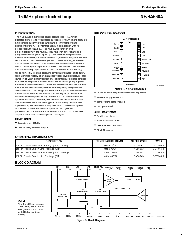
PIN CONFIGURATION
D, N Packages
VCC2 1 GND2 2 20 19 18 17 16 LF1 LF2 LF3 LF4 FREQ ADJ
GND1 3 TCAP1 TCAP2 GND1 4 5 6
15 OUT FILT 14 VOUT
VCC1 7 REFBYP PNPBYP 8 9
13 TCADJ2...