Ping Jing PJM7002NSA
N-Enhancement Field Effect Transistor
| Part No. | PJM7002NSA |
|---|---|
| Datasheet | PJM7002NSA Download |
| Manufacturer |  Ping Jing |
| Description | N-Enhancement Field Effect Transistor |
| Buy | Stock & Price |

FEATURES
● High density cell design for low RDS(ON)● Voltage controlled small signal switching
● High saturation current capability
● High speed switching SOT-23 Application
● PWM applications
● Load switch
● Power management Schematic diagram Drain 3
ABSOLUTE MAXIMUM RATINGS
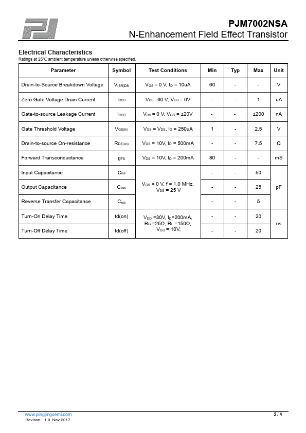
Ratings at 25℃ ambient temperature unless otherwise specified. Parameter Drain-Source Voltage Gate-Source Voltage Continuous Drain Current Pulsed Drain Current Total Power Dissipation Operating Junction Temperature Storage Temperature 1 Gate 2 Source Symbol VDS VGS ID IDM PD TJ TSTG Value 60 ± 20 115 800 200 150 - 55 to + 150 Unit V V mA mA mW OC OC Revison:1.0 Nov-2017 1/4 PJM7002NSA N-Enhancement Field Effect TransistorELECTRICAL CHARACTERISTICS
Ratings at 25℃ ambient temperature unless otherwise specified. Parameter Symbol Test Conditions Min Typ Max Unit Drain-to-Source Breakdown Voltage V(BR)DS VGS