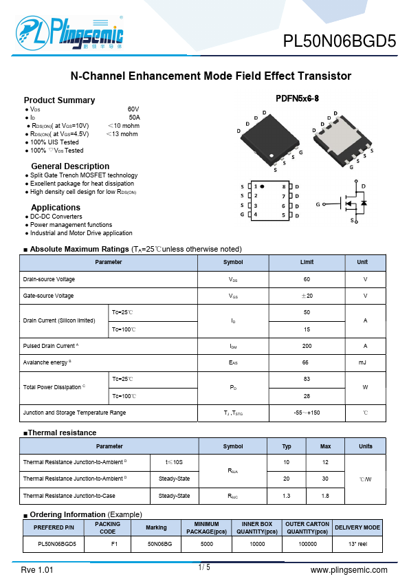
PL50N06BGD5
Description
- Split Gate Trench MOSFET technology
- Excellent package for heat dissipation
- High density cell design for low RDS(ON)
Applications
- DC-DC Converters
- Power management functions
- Industrial and Motor Drive application
- Absolute Maximum Ratings (TA=25℃unless otherwise noted)
Parameter
Symbol
Limit
Unit
Drain-source Voltage
Gate-source Voltage
±20
Drain Current (Silicon limited)
Tc=25℃ Tc=100℃
Pulsed Drain Current A Avalanche energy B
66 m J
Total Power Dissipation C
Tc=25℃ Tc=100℃
Junction and Storage Temperature Range
TJ ,TSTG
-55~+150
℃
- Thermal resistance
Parameter Thermal Resistance Junction-to-Ambient D Thermal Resistance Junction-to-Ambient D Thermal Resistance Junction-to-Case t≤10S Steady-State Steady-State
Symbol RθJA...