PO74G126A
PO74G126A is QUADRUPLE BUS BUFFER GATE manufactured by Potatosemi.
FEATURES
:
. Patented technology . Operating frequency up to 1.125GHz with 2pf load . Operating frequency up to 700MHz with 5pf load .. . Operating frequency up to 400MHz with 15pf load . VCC Operates from 1.65V to 3.6V . Propagation delay < 1.5ns max with 15pf load . Low input capacitance: 4pf typical . Available in 14pin 150mil wide SOIC package
DESCRIPTION
:
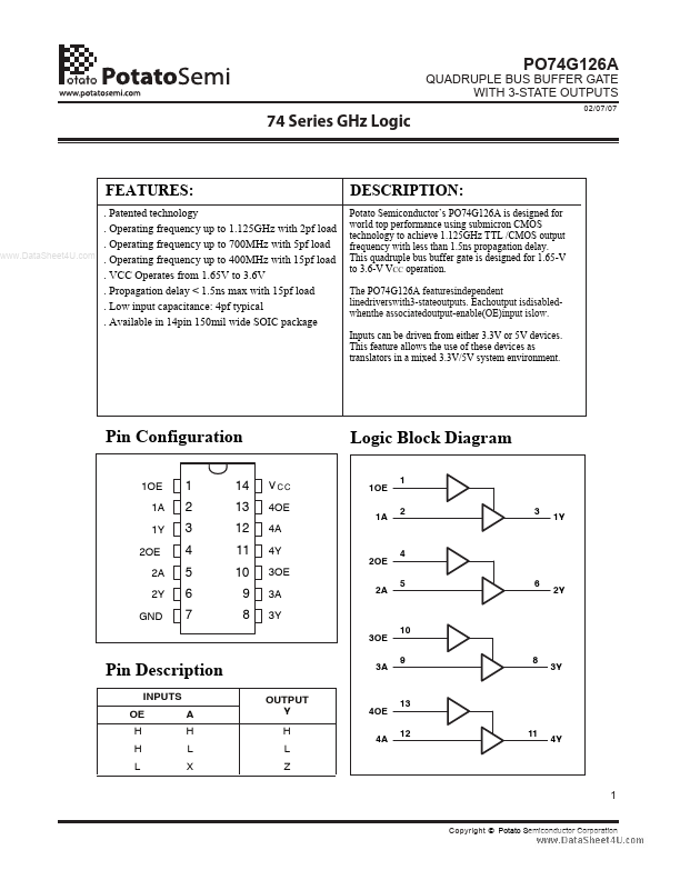
Potato Semiconductor’s PO74G126A is designed for world top performance using submicron CMOS technology to achieve 1.125GHz TTL /CMOS output frequency with less than 1.5ns propagation delay. This quadruple bus buffer gate is designed for 1.65-V to 3.6-V VCC operation. The PO74G126A featuresindependent linedriverswith3-stateoutputs. Eachoutput isdisabledwhenthe associatedoutput-enable(OE)input islow. Inputs can be driven from either 3.3V or 5V devices. This feature allows the use of these devices as translators in a mixed 3.3V/5V system environment.
Pin Configuration
1OE 1A 1Y 2OE 2A 2Y GND
Logic Block Diagram
VCC 4OE 4A 4Y
2OE 4 5 6 1OE 1A 1 2 3
1 2 3 4 5 6 7
14 13 12 11 10 9 8
1Y
3OE 3A 3Y
3OE 10 9 8 2A 2Y
Pin Description
INPUTS OE H H L A H L X OUTPUT Y H L Z
3A
3Y
4OE 4A
13 12 11
4Y
Copyright © Potato Semiconductor Corporation
QUADRUPLE BUS BUFFER GATE WITH 3-STATE OUTPUTS
02/07/07
74 Series GHz Logic
Maximum Ratings
Description
Storage Temperature
..
Max -65 to 150 -40 to 85 -0.5 to +4.6 -0.5 to +5.5 -0.5 to Vcc+0.5
Unit °C °C V V V
Note: stresses greater than listed under Maximum Ratings may cause permanent damage to the device. This is a stress rating only and functional operation of the device at these or any other conditions above those indicated in the operational sections of this specification is not implied. Exposure to absolute maximum rating conditions for extended periods may affect reliability specification is not implied.
Operation Temperature Operation Voltage Input Voltage Output Voltage
DC Electrical Characteristics
Symbol Description
Output High voltage...