SMP402
SMP402 is 20-72 VDC Input Non-isolated DC Output manufactured by Power Integrations.
Description
The SMP402, intended for non-isolated ISDN telemunications power supply applications, bines a high voltage power MOSFET switch with a switchmode power system controller in a monolithic integrated circuit. Few external ponents are required to implement a low cost power supply which meets stringent ISDN specifications. High frequency operation reduces total power supply size. The P-channel power MOSFET switch features include high voltage, low RDS(ON), and low capacitance. Lower capacitance results in a reduction in gate drive power, and also facilitates higher frequency operation. The controller section of the SMP402 contains all the blocks required to drive and control the power stage: start-up preregulator circuit, oscillator, bandgap reference, error amplifier, gate driver and level shift. Protection features include undervoltage lockout, thermal shutdown, and input polarity and level sensing. The SMP402 is available in a 16-pin plastic SOIC package.
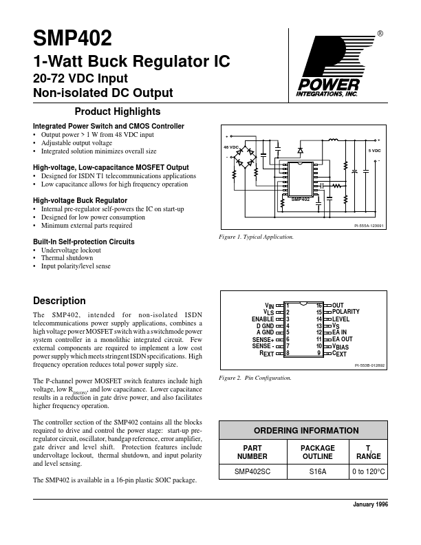
VIN VLS ENABLE D GND A GND SENSE+ SENSE REXT
1 2 3 4 5 6 7 8
16 15 14 13 12 11 10 9
OUT POLARITY LEVEL VS EA IN EA OUT VBIAS CEXT
PI-553B-012892
Figure 2. Pin Configuration.
ORDERING INFORMATION
PART NUMBER SMP402SC PACKAGE OUTLINE S16A Tj RANGE 0 to 120°C
January 1996
VIN VLS ENABLE VBIAS VS A GND REXT D GND S CEXT EA OUT
+
HV REG
UV LOCKOUT VREF BANDGAP REF THERMAL SHUTDOWN LEVEL SHIFT
+
- R
PWM PARATOR
EA IN
- ERROR AMPLIFIER
4V
+
23 µA 5 µA
SENSE+ LEVEL
POLARITY
23 µA 5 µA
SENSE-
PI-552B-062293
Figure 3. Functional Block Diagram.
D 1/96
SMP402 Pin Functional Description
Pin 1: VIN is the high-voltage input to the switching regulator. This is the Source connection of the P-Channel power MOSFET pass transistor. Pin 2: VLS is an internal supply for the level shift circuit that drives the P-Channel MOSFET. A capacitor should be placed between VLS and VIN for bypassing. V LS is normally 10 V below VIN . Pin 3: The power supply can be shut...