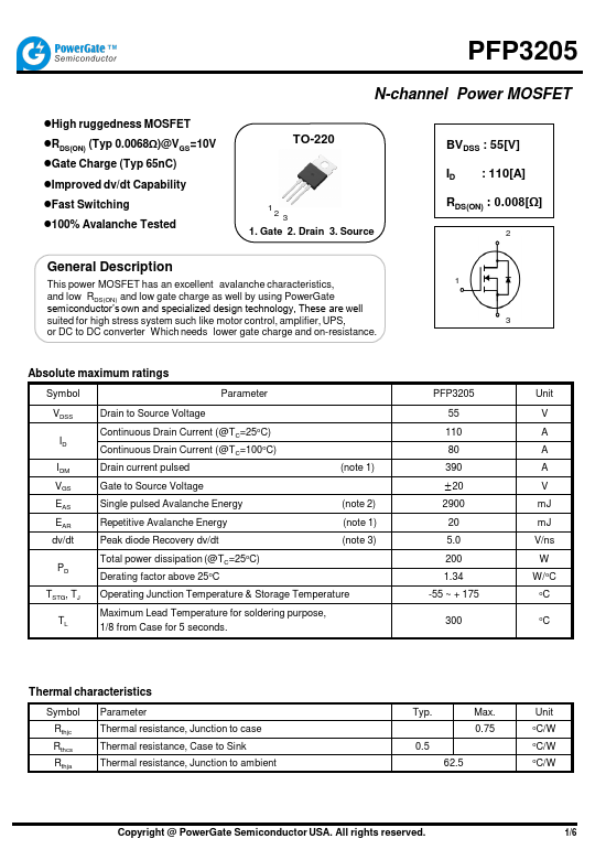
GENERAL DESCRIPTION
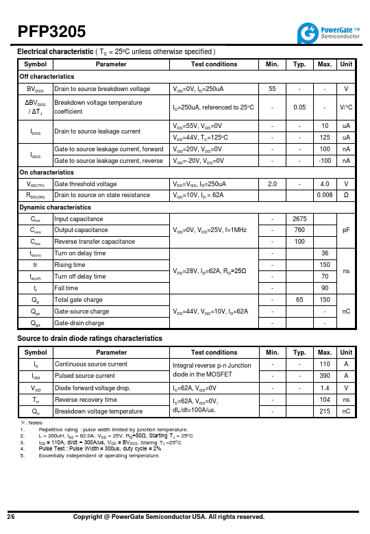
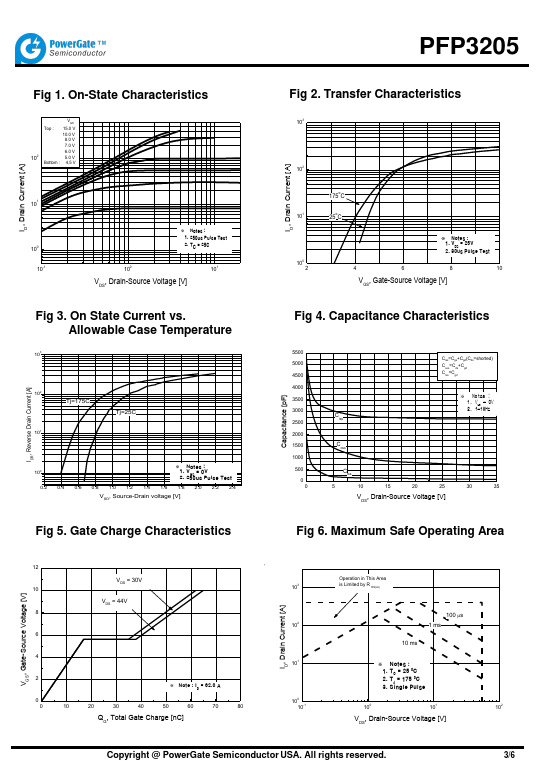
1 3 Absolute maximum ratings Symbol Parameter VDSS ID IDM VGS EAS EAR dv/dt PD TSTG, TJ TL Drain to Source Voltage Continuous Drain Current (@TC=25oC) Continuous Drain Current (@TC=100oC) Drain current pulsed (note 1) Gate to Source Voltage Single pulsed Avalanche Energy (note 2) Repetitive Avalanche Energy (note 1) Peak diode Recovery dv/dt (note 3) Total power dissipation (@TC=25oC) Derating factor above 25oC Operating Junction Temperature & Storage Temperature Maximum Lead Temperature for soldering purpose, 1/8 from Case for 5 seconds. PFP3205 55 110 80 390 ±20 2900 20 5.0 200 1.34 -55 ~ + 175 300 Unit V A A A V mJ mJ V/ns W W/oC oC oC Thermal characteristics Symbol Rthjc Rthcs Rthja Parameter Thermal resistance, Junction to case Thermal resistance, Case to Sink Thermal resistance, Junction to ambient Typ. Max. 0.75 0.5 62.5 Unit oC/W oC/W oC/W Copyright @ PowerGate Semiconductor USA. All rights reserved. 1/6 PFP3205 Electrical characteristic ( TC = 25oC unless o...