PDPM6N20V3
PDPM6N20V3 is P-Channel MOSFET manufactured by Prisemi.
Description
The enhancement mode MOS is extremely high density cell and low on-resistance.
PDPM6N20V3 P-Channel MOSFET
VDS(V) -20
MOSFET Product Summary
RDS(on)(mΩ)
ID(A)
110 @ VGS=-4.5V
-3
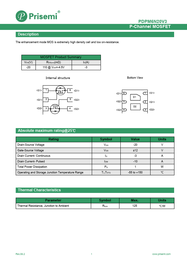
Internal structure
(S1) 1 (G1) 2 (D2) 3
6 (D1) 5 (G2) 4 (S2)
Bottom View
(D1) 6
1 (S1)
D1
(G2) 5
2 (G1)
(S2) 4
D2 3...