PPM3FD20V1EN
Description
The MOSFET provide the best bination of fast switching, low on-resistance and cost-effectiveness.
VDS(V) -20
MOSFET Product Summary
RDS(on)(Ω)
ID(m A)
0.45@ VGS=-4.5V
0.62@ VGS=-2.5V
-800
0.86@ VGS=-1.8V
PPM3FD20V1EN P-Channel MOSFET
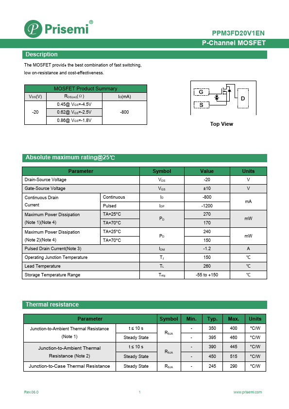
Top View
Absolute maximum rating@25℃
Parameter
Drain-Source Voltage Gate-Source Voltage Continuous Drain Current
Maximum Power Dissipation (Note 1)(Note 4)
Maximum Power Dissipation (Note 2)(Note 4) Pulsed Drain Current(Note 3) Operating Junction Temperature Lead Temperature Storage Temperature Range
Continuous Pulsed TA=25°C TA=70°C TA=25°C TA=70°C
Symbol
VDS VGS ID IDP
IDM TJ TL Tstg
Value
-20 ±10 -800 -1200 270 170 240 150 -1.2 150 260 -55 to +150
Units
V V m A m W m W A ℃ ℃ ℃
Thermal resistance
Parameter
Junction-to-Ambient Thermal Resistance (Note 1)
Junction-to-Ambient Thermal Resistance (Note 2)
Junction-to-Case Thermal Resistance t ≤ 10 s Steady State t ≤ 10 s Steady State Steady State
Symbol
RθJA
RθJA RθJA
Min.
-...