PSM6N30V20
Description
The PSM6N30V20 uses split gate trench technology to provide excellent Rdson low gate charge. This device is suitable for power management and high efficiency applications at high switching frequencies applications.
MOSFET Product Summary
VDS(V) 30
RDS(on)(mΩ) 4.0 @ VGS = 10V
ID(A) 20
Feature
- High Power and current handing capability
- Lead free product is acquired
- Surface Mount Package
Applications
- PWM applications
- Load switch
- Power management
- DC-DC Converters
- Wireless Chargers
Absolute maximum rating@25℃
Rating Drain-source Voltage Gate-source Voltage Drain Current Pulsed Drain Current1) Avalanche Energy, Single Pulse Total Power Dissipation2) Thermal Resistance Junction-to-Ambient @ Steady State2) Junction and Storage Temperature Range
PSM6N30V20 N-Channel MOSFET
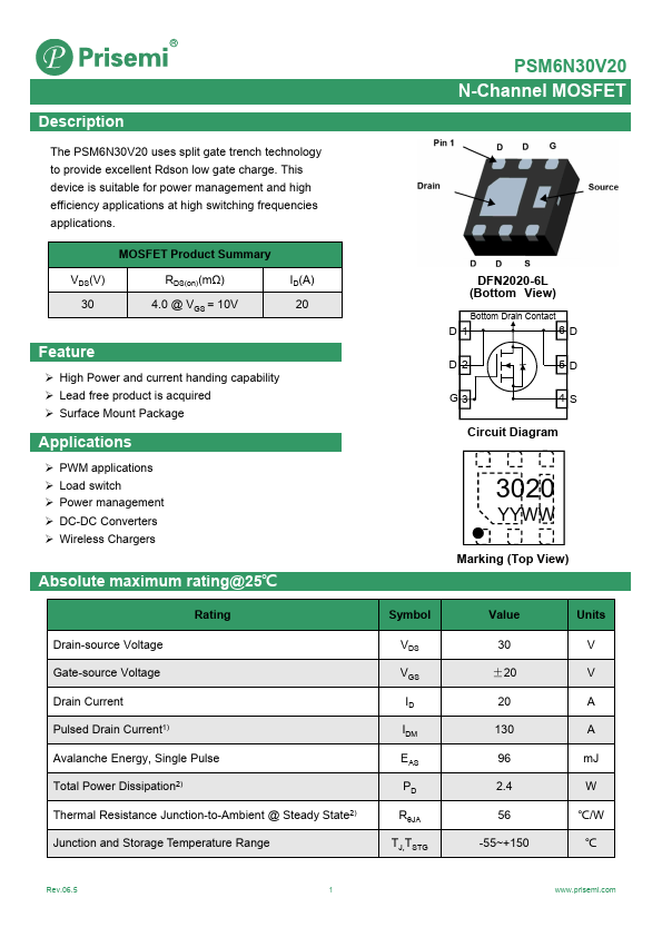
DFN2020-6L (Bottom View)
Bottom Drain Contact
D1
6D
D2
5D
G3
4S
Circuit Diagram
YYWW
Marking (Top View)
Symbol VDS VGS ID IDM EAS PD RθJA
TJ,TSTG
Value 30
±20 20 130 96 2.4...