V58C2512164SBI5
V58C2512164SBI5 is High Performance 512M-Bit DDR SDRAM manufactured by ProMOS Technologies.
..
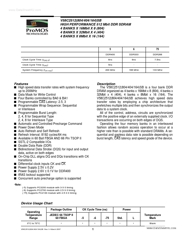
V58C2512(804/404/164)SB HIGH PERFORMANCE 512 Mbit DDR SDRAM 4 BANKS X 16Mbit X 8 (804) 4 BANKS X 32Mbit X 4 (404) 4 BANKS X 8Mbit X 16 (164)
5 DDR400 Clock Cycle Time (tCK2.5) Clock Cycle Time (tCK3) System Frequency (fCK max) 6ns 5ns 200 MHz
6 DDR333 6ns 166 MHz
75 DDR266 7.5ns 133 MHz
Features
- High speed data transfer rates with system frequency up to 200MHz
- Data Mask for Write Control
- Four Banks controlled by BA0 & BA1
- Programmable CAS Latency: 2.5, 3
- Programmable Wrap Sequence: Sequential or Interleave
- Programmable Burst Length: 2, 4, 8 for Sequential Type 2, 4, 8 for Interleave Type
- Automatic and Controlled Precharge mand
- Power Down Mode
-...