PulseCore Semiconductor PCS3P2191A
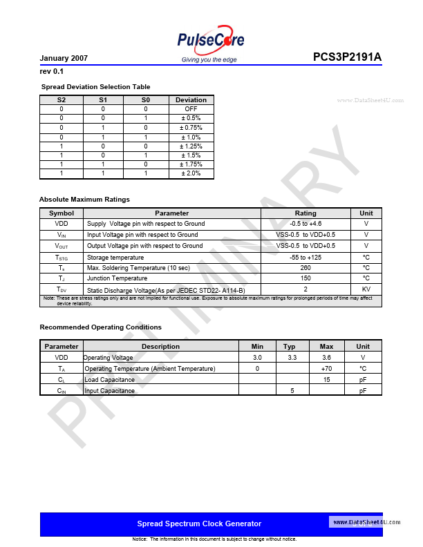
The PCS3P2191A allows significant system cost savings by reducing the number of circuit board layers, ferrite beads, and shielding that are traditionally required to pass EMI regulations. The PCS3P2191A uses the most efficient and optimized modulation profile approved by the FCC and is implemented in a proprietary all digital method. January 2007 rev 0.1 Spread Spectrum Clock Generator Features • • • • • PCS3P2191A offers seven selectable centre spread options of ±0.5% to ±2.0%, and a no spread option.| Part No. | PCS3P2191A |
|---|---|
| Datasheet | PCS3P2191A Download |
| Manufacturer | PulseCore Semiconductor |
| Description | Spread Spectrum Clock Generator |
| Buy | Stock & Price |
DESCRIPTION
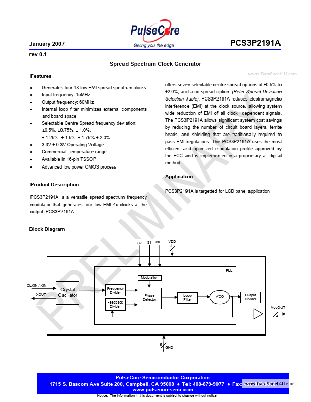
PCS3P2191A is targetted for LCD panel application PCS3P2191A is a versatile spread spectrum frequency modulator that generates four low EMI 4x clocks at the output. PCS3P2191A Block Diagram S2 S1 S0 VDD 2 PLL Modulation CLKIN / XIN XOUT Crystal Oscillator Frequency Divider Feedback Divider Phase Detector Loop Filter VCO Output Divider ModOUT 4 5 GND PulseCore Semiconductor Corporation 1715 S. Bascom Ave Suite 200, Campbell, CA 95008● Tel: 408-879-9077
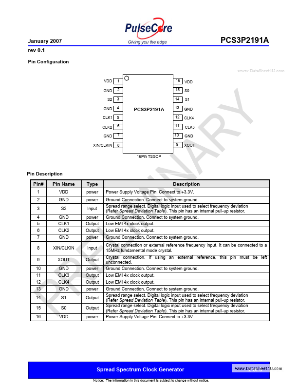
● Fax: 408-879-9018 Notice: The information in this document is subject to change without notice. January 2007 rev 0.1 Pin Configuration PCS3P2191A VDD GND S2 GND CLK1 CLK2 GND XIN/CLKIN 1 2 3 4 5 6 7 8 16Pin TSSOP 16 15 14 VDD S0 S1 GND CLK4 CLK3 GND XOUT PCS3P2191A 13 12 11 10 9 Pin
DESCRIPTION
Pin# 1 2 3 4 5 6 7 8 9 10 11 12 13 14 15 16 Pin Name VDD GND S2 GND CLK1 CLK2 GND XIN/CLKIN XOUT GND CLK3 CLK4 GND S1 S0 VDD Type power power Input power Output Output power Input Output power Output Output power Output Output powerDESCRIPTION
Power Supply Voltage Pin.