PCS3P622Z09C
Description
External reference Clock input, 5V tolerant input CLKOUT1 GND CLKOUT22 CLKOUT3 VDD CLKOUT4 2 2 DLY_CTRL External Input-Output Delay control. This pin can be used as clock output4 Low Frequency Timing-Safe™ Peak EMI Reduction IC Notice: The information in this document is subject to change without notice. 3 of 15.
Key Features
- Low Frequency Clock distribution with TimingSafe™ Peak EMI Reduction Input frequency range: 4MHz - 20MHz Multiple low skew Timing-safe™ Outputs: PCS3P622Z05: 5 Outputs PCS3P622Z09: 9 Outputs * * *
- External Input-Output Delay Control option Supply Voltage: 3.3V±0.3V Commercial and Industrial temperature range Packaging Information: ASM3P622Z05: 8 pin SOIC, and TSSOP ASM3P622Z09:16 pin SOIC, and TSSOP
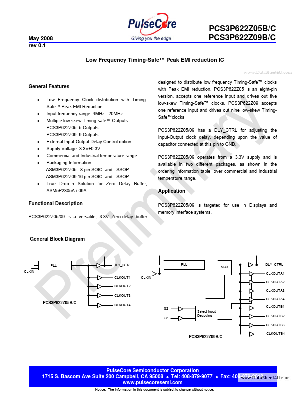
- True Drop-in Solution for Zero Delay Buffer, ASM5P2305A / 09A designed to distribute low frequency Timing-Safe™ clocks with Peak EMI reduction. PCS3P622Z05 is an eight-pin version, accepts one reference input and drives out five low-skew Timing-Safe™ clocks. PCS3P622Z09 accepts one reference input and drives out nine low-skew TimingSafe™clocks. PCS3P622Z05/09 has a DLY_CTRL for adjusting the Input-Output clock delay, depending upon the value of capacitor connected at this pin to GND. PCS3P622Z05/09 operates from a 3.3V supply and is available in two different packages, as shown in the ordering information table, over commercial and Industrial temperature range.