Datasheet4U Logo Datasheet4U.com

ASM2I99456 - 3.3V/2.5V LVCMOS Clock Fanout Buffer

General Description

The ASM2I99456 is a 2.5V and 3.3V compatible 1:10 clock distribution buffer designed for low-Voltage mid-range to high-performance telecom, networking and computing applications.

Both 3.3V, 2.5V and dual supply voltages are supported for mixed-voltage applications.

Key Features

  • Configurable 10 outputs LVCMOS Clock distribution buffer.
  • Compatible to single, dual and mixed 3.3V/2.5V Voltage supply.
  • Wide range output clock frequency up to 250MHz.
  • Designed for mid-range to high-performance telecom, networking and computer.

📥 Download Datasheet

Datasheet Details

Part number ASM2I99456
Manufacturer PulseCore
File Size 548.62 KB
Description 3.3V/2.5V LVCMOS Clock Fanout Buffer
Datasheet download datasheet ASM2I99456 Datasheet

Full PDF Text Transcription (Reference)

The following content is an automatically extracted verbatim text from the original manufacturer datasheet and is provided for reference purposes only.

View original datasheet text
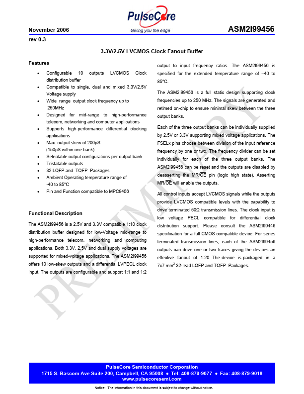
November 2006 rev 0.3 ASM2I99456 3.3V/2.5V LVCMOS Clock Fanout Buffer Features • Configurable 10 outputs LVCMOS Clock distribution buffer • Compatible to single, dual and mixed 3.3V/2.5V Voltage supply • Wide range output clock frequency up to 250MHz • Designed for mid-range to high-performance telecom, networking and computer applications • Supports high-performance differential clocking applications • Max. output skew of 200pS (150pS within one bank) • Selectable output configurations per output bank • Tristatable outputs • 32 LQFP and TQFP Packages • Ambient Operating temperature range of -40 to 85°C • Pin and Function compatible to MPC9456 Functional Description The ASM2I99456 is a 2.5V and 3.