PulseCore ASM2P2310A
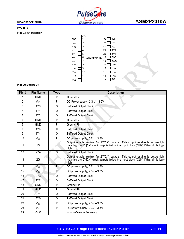
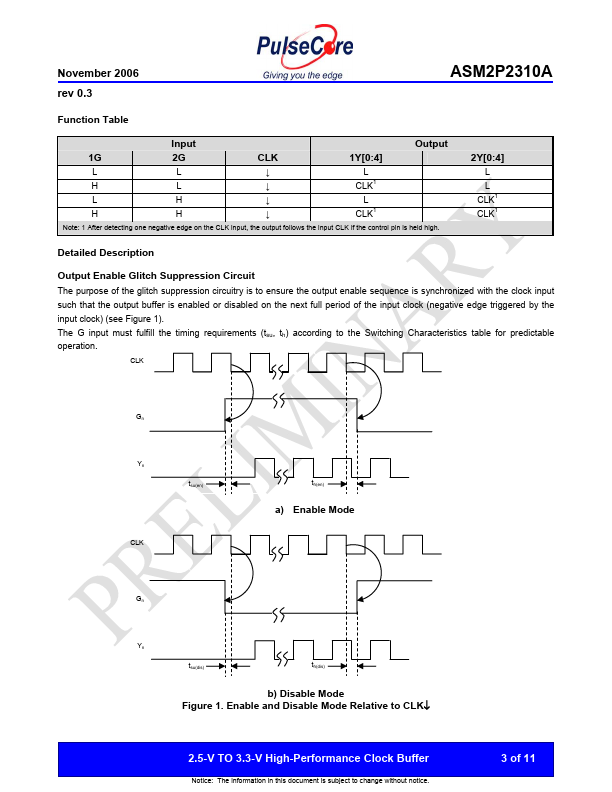
The ASM2P2310A is a high-performance, low-skew clock buffer that operates up to 200MHz. For normal operation, the outputs of bank 1Y[0:4] or 2Y[0:4] can be placed in a low state when the control pins (1G or 2G, respectively) are held low and a negative clock edge is detected on the CLK input. The outputs of bank 1Y[0:4] or 2Y[0:4] can be switched into the buffer mode when the control pins (1G and 2G) are held high and a negative clock edge is detected on the CLK input.| Part No. | ASM2P2310A |
|---|---|
| Datasheet | ASM2P2310A Download |
| Manufacturer | PulseCore |
| Description | 2.5-V TO 3.3-V High-Performance Clock Buffer |
| Buy | Stock & Price |
FEATURES
● High-Performance 1:10 Clock Driver for General Purpose applications. Operates up to 200 MHz at 3.3V Supply Voltage● Pin-to-Pin Skew < 100 pS at 3.3V Supply Voltage
● Supply Range : 2.3V to 3.6V
● Operating Temperature Range : -40°C to 85°C
● Output Enable Glitch Suppression
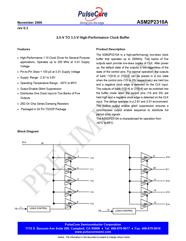
● Distributes One Clock Input to Two Banks of Five Outputs
● 25Ω On Chip Series Damping Resistors
● Packaged in 24 Pin TSSOP Package Block Diagram Product
DESCRIPTION
Two banks of five outputs each provide low-skew copies of CLK. After power up, the default state of the outputs is low regardless of the state of the control pins. The device operates in a 2.5V and 3.3V environment. The built-in output enable glitch suppression ensures a synchronized output enable sequence to distribute full period clock signals. The ASM2P2310A is characterized for operation from -40°C to 85°C. CLK 24 1G 11 LOGIC CONTROL 25Ω 25Ω 25Ω 25Ω 25Ω 3 4 5 8 9 1Y0 1Y1 1Y2 1Y3 1Y4 2G 13 LOGIC CONTROL 25Ω 25Ω 25Ω 25Ω 25Ω 21 20 17 16 12 2Y0 2Y1 2Y2 2Y3 2Y4 PulseCore Semiconductor Corporation 1715 S.