QL3012
QL3012 is qASIC 3 FPGA manufactured by QuickLogic.
. U 4 QL3012 p ASIC 3 FPGA Data Sheet t e e h S
- -
- -
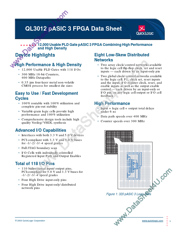
- - 12,000 Usable PLD Gate p ASIC 3 FPGA bining High Performance a t a and High Density Eight Low-Skew Distributed Device .D Highlights w Networks w Two array clock/control networks available Performance & High Density w High to the logic cell flip-flop clock, set and reset 12,000 Usable PLD Gates with 118 I/Os
- -
- 300 MHz 16-bit Counters, m o c
400 MHz Datapaths
- 0.35 µm four-layer metal non-volatile CMOS process for smallest die sizes
Easy to Use / Fast Development Cycles
- 100% routable with 100% utilization and inputs
- each driven by an input-only pin
- Two global clock/control networks available to the logic cell; F1, clock set, reset inputs and the input, I/O register clock, reset, and enable inputs as well as the output enable control
- each driven by an input-only or I/O pin, or any logic cell output or I/O cell feedback plete pin-out stability
- Variable-grain logic cells provide high performance and 100% utilization
- prehensive design tools include high quality Verilog/VHDL synthesis
Advanced I/O Capabilities
- Interfaces with both 3.3 V and 5.0 V devices
- PCI pliant with 3.3 V and 5.0 V buses for -1/-2/-3/-4 speed grades
- Full JTAG boundary scan
- I/O Cells with individually controlled Registered Input Path and Output Enables
Total of 118 I/O Pins
- 110 bidirectional input/output pins,
PCI-pliant for 5.0 V and 3.3 V buses for -1/-2/-3/-4 speed grades
- Four High Drive input-only pins
- Four High Drive input-only/distributed network pins w w w
.D t a
S a e h
High Performance
- Input + logic cell + output total delays under 6 ns
- Data path speeds over 400...