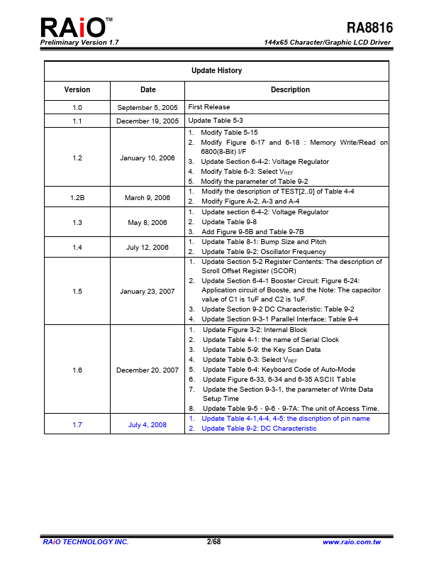
DESCRIPTION
September 5, 2005 December 19, 2005 January 10, 2006 March 9, 2006 May 8, 2006 July 12, 2006 January 23, 2007 December 20, 2007 July 4, 2008 First Release Update Table 5-3 1. Modify Table 5-15 2. Modify Figure 6-17 and 6-18 : Memory Write/Read on 6800(8-Bit) I/F 3. Update Section 6-4-2: Voltage Regulator 4. Modify Table 6-3: Select VREF 5. Modify the parameter of Table 9-2 1. Modify the description of TEST[2..0] of Table 4-4 2. Modify Figure A-2, A-3 and A-4 1. Update section 6-4-2: Voltage Regulator 2. Update Table 9-8 3. Add Figure 9-5B and Table 9-7B 1. Update Table 8-1: Bump Size and Pitch 2. Update Table 9-2: Oscillator Frequency 1. Update Section 5-2 Register Contents: Update Section 6-4-1 Booster Circuit: Figure 6-24: Application circuit of Booste, and the Note: The capacitor value of C1 is 1uF and C2 is 1uF. 3. Update Section 9-2 DC Characteristic: Table 9-2 4. Update Section 9-3-1 Parallel Interface: Table 9-4 1. Update Figure 3-2: Internal Block 2. Update Table 4-1: the name of Serial Clock 3. RAIO Technology