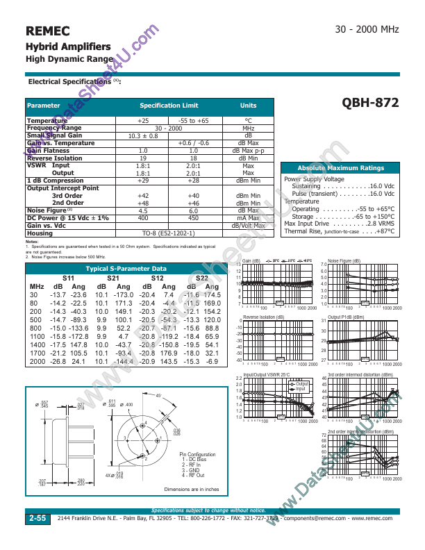
Parameter Temperature Frequency Range Small Signal Gain Gain vs. Temperature Gain Flatness Reverse Isolation VSWR Input Output 1 dB Compression Output Intercept Point 3rd Order 2nd Order Noise Figure (2) DC Power @ 15 Vdc ± 1% Gain vs. Vdc Housing w w a D . w S a t e: e h (1) U 4 t .c om 30 - 2000 MHz Specification Limit -55 to +65 30 - 2000 10.3 ± 0.8 +0.6 / -0.6 1.0 1.0 19 18 1.8:1 2.0:1 1.8:1 2.0:1 +29 +28 +42 +48 4.5 400 +40 +46 6.0 450 +25 Units °C MHz dB dB Max dB Max p-p dB Min Max Max dBm Min dBm Min dBm Min dB Max mA Max dB/Volt Max QBH-872
ABSOLUTE MAXIMUM RATINGS
Power Supply Voltage Sustaining . . . . . . . . . . . .16.0 Vdc Pulse (transient) . . . . . . . .16.0 Vdc Temperature Operating . . . . . . . . .-55 to +65°C Storage . . . . . . . . . .-65 to +150°C Max Input Drive . . . . . . . . .2.8 VRMS Thermal Rise, junction-to-case . . . .+87°C TO-8 (E52-1202-1) Notes: 1. Specifications are guaranteed when tested in a 50 Ohm system. Specifications indicated as typical are not guaranteed.
This website uses cookies or similar technologies, to enhance your browsing experience and provide personalized recommendations. By continuing to use our website, you agree to our Privacy Policy