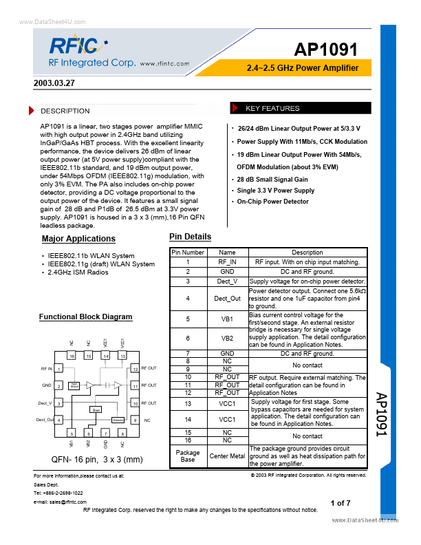
AP1091
AP1091 is Power Amplifier manufactured by RFIC.
features a small signal gain of 28 d B and P1d B of 26.5 d Bm at 3.3V power supply. AP1091 is housed in a 3 x 3 (mm),16 Pin QFN leadless package.
- 26/24 d Bm Linear Output Power at 5/3.3 V
- Power Supply With 11Mb/s, CCK Modulation
- 19 d Bm Linear Output Power With 54Mb/s, OFDM Modulation (about 3% EVM)
- 28 d B Small Signal Gain
- Single 3.3 V Power Supply
- On-Chip Power Detector
Major Applications
- IEEE802.11b WLAN System
- IEEE802.11g (draft) WLAN System
- 2.4GHz ISM Radios
Pin Details
Pin Number 1 2 3 4 Name RF_IN GND Dect_V Dect_Out VB1 VB2 GND NC NC RF_OUT RF_OUT RF_OUT VCC1 VCC1 NC NC Description
RF input. With on chip input matching. DC and RF ground. Supply voltage for on-chip power detector. Power detector output. Connect one 5.6kΩ resistor and one 1u F capacitor from pin4 to ground. Bias current control voltage for the first/second stage. An external resistor bridge is necessary for single voltage supply application. The detail configuration can be found in Application Notes. DC and RF ground. No contact RF output. Require external matching. The detail configuration can be found in Application Notes Supply voltage for first stage. Some bypass capacitors are needed for system application. The detail configuration can be found in Application Notes. No contact
Functional Block Diagram
VCC1 VCC1
5 6 7 8 9 10 11 12 13 14 15 16 Package Base
16 RF IN 1
NC 15
13 12 RF OUT
Input Match
11 RF OUT
Dect_V
Bias
10 RF OUT
Dect_Out 4 5 VB1 6 VB2 7 GND
Detector
8 NC
QFN- 16 pin, 3 x 3 (mm)
For more information,please contact us at: Sales Dept. Tel: +886-2-2698-1022 e-mail: sales@rfintc.
The package ground provides circuit Center Metal ground as well as heat dissipation path for the power amplifier.
© 2003 RF Integrated Corporation. All rights reserved.
RF integrated Corp. reserved the right to make any changes to the specifications without notice.
1 of...