VRS51C1100
VRS51C1100 is Versa 8051 MCU manufactured by Ramtron.
Overview
The VRS51C1100 is based on the standard 8051 microcontroller architecture and is a pin patible drop-in replacement for the 8051. The VRS51C1100 is aimed at a diversity of applications that require a large amount of program/data memory with non-volatile data storage and/or code/field based firmware upgrade capability coupled with prehensive peripheral support. It features
64KB of In-System/In-Application Programmable Flash memory, 64KB Data Flash memory, 1KB of RAM, 4 PWM outputs, a UART, three 16-bit timers/counters, a watchdog timer and power down features
. The VRS51C1000 is available with firmware that enables In-System Programming (firmware based bootloader) of the Flash memory via the UART interface (ISPVx version). General Flash memory programming is supported by device programmers available from Ramtron or other 3rd party mercial programmer suppliers. The VRS51C1100 is available in PLCC-44, QFP-44 and DIP-40 packages and functions over the industrial temperature range.
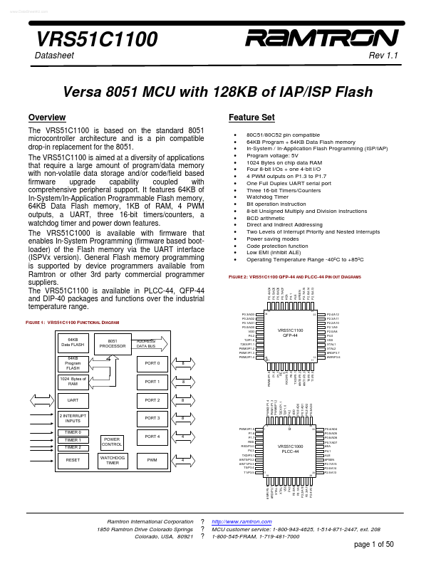
FIGURE 1: VRS51C1100 FUNCTIONAL DIAGRAM
Feature
Set
- -
- -
- -
- -
- -
- -
- -
- -
- -
- 80C51/80C52 pin patible 64KB Program + 64KB Data Flash memory In-System / In-Application Flash Programming (ISP/IAP) Program voltage: 5V 1024 Bytes on chip data RAM Four 8-bit I/Os + one 4-bit I/O 4 PWM outputs on P1.3 to P1.7 One Full Duplex UART serial port Three 16-bit Timers/Counters Watchdog Timer Bit operation instruction 8-bit Unsigned Multiply and Division instructions BCD arithmetic Direct and Indirect Addressing Two Levels of Interrupt Priority and Nested Interrupts Power saving modes Code protection function Low EMI (inhibit ALE) Operating Temperature Range -40ºC to +85ºC
FIGURE 2: VRS51C1100 QFP-44 AND PLCC-44 PIN OUT DIAGRAMS
P0.4/AD4 P0.5/AD5 P0.6/AD6 P0.7/AD7 #EA #PSEN P2.7/A15 P2.6/A14 P2.5/A13
23 22
P0.3/AD3 P0.2/AD2 P0.1/AD1 P0.0/AD0 VDD
P4.1 ALE
P2.4/A12 P2.3/A11 P2.2/A10
64KB Data FLASH 64KB Program FLASH 1024 Bytes of RAM
8051 PROCESSOR
ADDRESS/ DATA BUS
P4.2...