Datasheet Summary
DDR/SDRAM Buffer
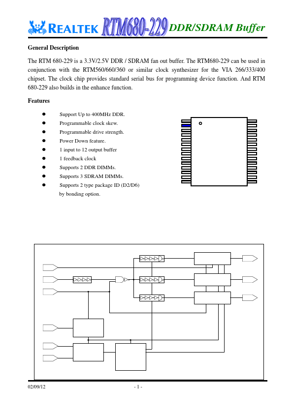
General Description The RTM 680-229 is a 3.3V/2.5V DDR / SDRAM fan out buffer. The RTM680-229 can be used in conjunction with the RTM560/660/360 or similar clock synthesizer for the VIA 266/333/400 chipset. The clock chip provides standard serial bus for programming device function. And RTM 680-229 also builds in the enhance function. Features z z z z z z z z z Support Up to 400MHz DDR. Programmable clock skew. Programmable drive strength. Power Down feature. 1 input to 12 output buffer 1 feedback clock Supports 2 DDR DIMMs. Supports 3 SDRAM DIMMs. Supports 2 type package ID (D2/D6) by bonding option.
Delay select
DDR#/SDRAM PAD
CLK OUT
DDR#/SDRAM clk_in
Delay...