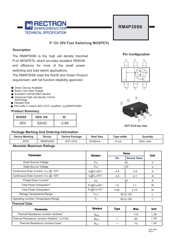
DESCRIPTION
Pin Configuration Green Device Available Super Low Gate Charge Excellent CdV/dt effect decline Advanced high cell density Trench technology Halogen-free P/N suffix V means AEC-Q101 qualified, e.g:RM4P30S6V Product Summary BVDSS RDS ON ID -30V 52mΩ -3.9A Package Marking And Ordering Information Device Marking Device Device Package 4P30 RM4P30S6 SOT-23-6 ABSOLUTE MAXIMUM RATINGS
Reel Size Ø180mm DS D DG D SOT-23-6 top view Tape width 8 mm Quantity 3000 units Drain-Source Voltage Gate-SouUce Voltage Continuous Drain Current, VGS @ -10V1 Continuous Drain Current, VGS @ -10V1 Pulsed Drain Current2 Total Power Dissipation3 Total Power Dissipation3 Storage Temperature Range Operating Junction Temperature Range Thermal Data Thermal Resistance Junction Ambient 1 Thermal Resistance Junction-Ambient 1 (t ≤10s) Thermal Resistance Junction-Case1 VDS VGS ID@TA=25ć ID@TA =70ć IDM PD@TA=25ć PD@TA= 70ć TSTG TJ RθJA RθJA RθJC 10s S teady State -30 V f20 V -4.5 -3.9 A -3.5 -3.1 A -20 A 1.5 1. Rectron Semiconductor