HD26LS32A
HD26LS32A is Quadruple Differential Line Receivers manufactured by Renesas.
Description
The HD26LS32A features quadruple line receivers designed to meet the specs of EIA standard RS-422A and RS-423. This device operates from a single 5 V power supply. The enable function is mon to all four receivers and offers a choice of active high or active low input. Fail safe design ensures that if the inputs are open, the outputs will always be high.
Features
- Ordering Information
Part Name HD26LS32AP Package Type Package Code P Package Abbreviation
- Taping Abbreviation (Quantity)
DILP-16 pin (JEITA) DP-16E, -16FV
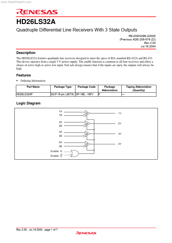
Logic Diagram
1A 1B 2A 2B 3A 3B 4A 4B Enable G Enable G 1Y
2Y
3Y
4Y
Rev.2.00, Jul.16.2004, page 1 of 7
..
Pin Arrangement
1B 1 1A 2 1Y 3 Enable G 4 2Y 5 2A 6 2B 7 GND 8
16 VCC 15 4B 14 4A 13 4Y 12 Enable G 11 3Y 10 3A 9 3B
(Top view)
Function Table
Differential Input A- B VID≥ V TH VTL < VID < VTH VID≤ V TL X H L X ? Z : : : : : High level Low level Immaterial Irrelevant High impedance H X H X H X L Enable G X L X L X L H G H H ? ? L L Z Output Y
Absolute Maximum Ratings
Item
Symbol
Ratings
Unit
Supply Voltage VCC- 7.0 V Input Voltage A or B VIN ±25 V Differential Input Voltage VID- 2 ±25 V Enable Input Voltage VIN 7 V Output Sink Current Iout 50 m A Continuous Total Dissipation PT 1 W Operating Temperature Topr 0 to +70 °C Storage Temperature Tstg
- 65 to 150 °C Notes: 1. All voltage values except for differential input voltage are with respect to network ground terminal. 2. Differential input voltage is measured at the noninverting input with respect to the corresponding inverting input. 3. The absolute maximum ratings are values which must not individually be exceeded, and furthermore, no two of which may be realized at the same time.
Rev.2.00, Jul.16.2004, page 2 of 7
..
Remended Operating Conditions
Item Supply Voltage In Phase Input Voltage Output Current Operating Temperature Symbol VCC VIC IOH IOL Topr 4.75
- -
- 0 Min 5.00
- -
- - Typ Max 5.25 ±7.0
- 440 8 70 V V µA m A °C Unit
Electrical...