HD74LV1GT126A Description
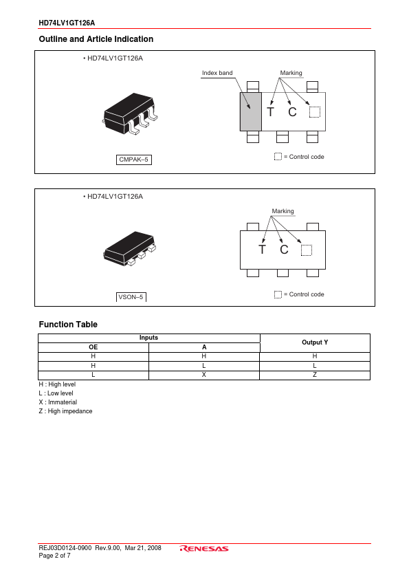
The HD74LV1GT126A has a bus buffer gate with 3 state output in a 5 pin package. Output is disabled when the associated output enable (OE) input is low. To ensure the high impedance state during power up or power down, OE should be connected to VCC through a pull-down resistor;.
HD74LV1GT126A Key Features
- The basic gate function is lined up as Renesas uni logic series
- Supplied on emboss taping for high-speed automatic mounting
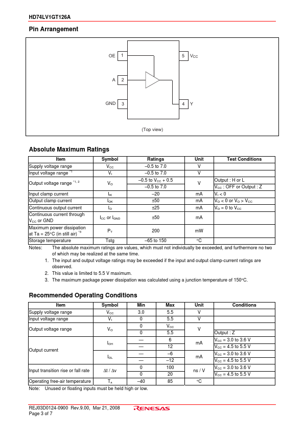
- TTL patible input level. Supply voltage range : 3.0 to 5.5 V Operating temperature range : -40 to +85°C
- Logic-level translate function 3.0 V CMOS logic → 5.0 V CMOS logic (@VCC = 5.0 V) 1.8 V or 2.5 V CMOS logic → 3.3 V CMOS
- All inputs VIH (Max.) = 5.5 V (@VCC = 0 V to 5.5 V) All outputs VO (Max.) = 5.5 V (@VCC = 0 V, Output : Z)
- Output current ±6 mA (@VCC = 3.0 V to 3.6 V), ±12 mA (@VCC = 4.5 V to 5.5 V)
- All the logical input has hysteresis voltage for the slow transition
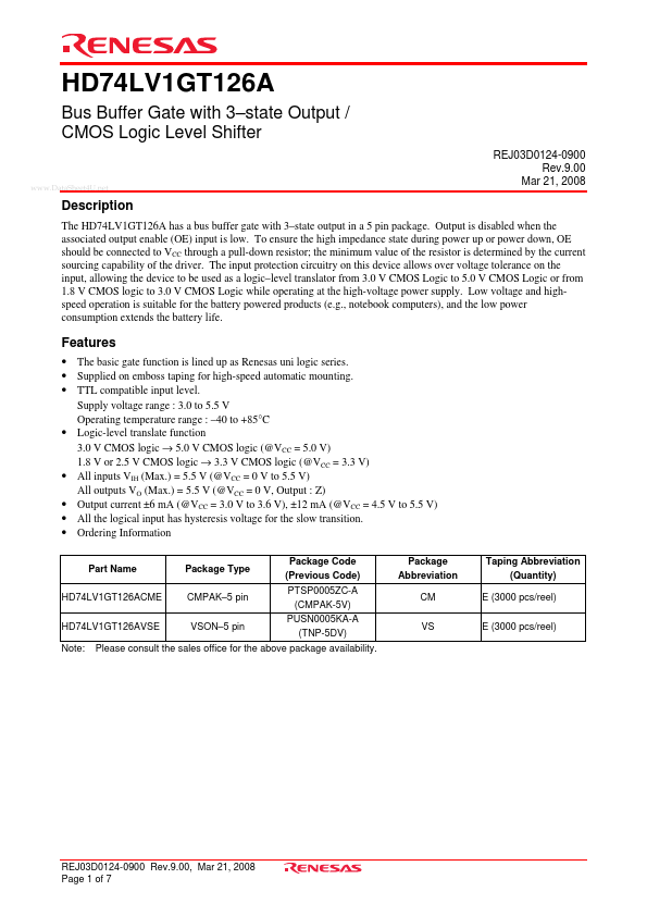
- Ordering Information
- HD74LV1GT126A
- HD74LV1GT126A