HD74LV2G245A Description
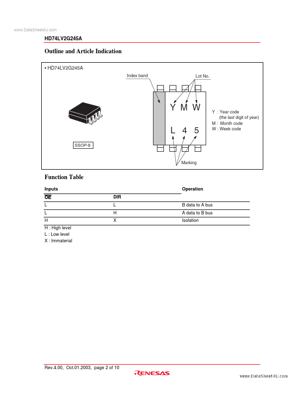
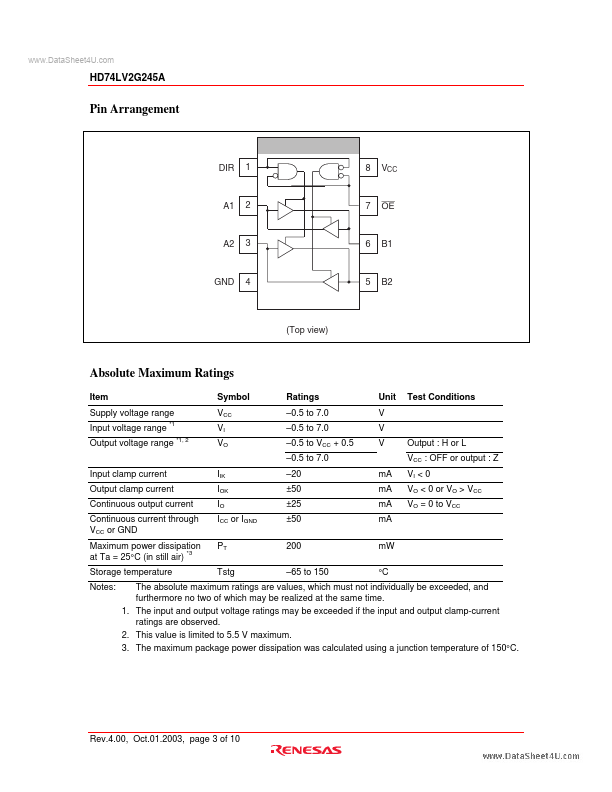
The HD74LV2G245A has two buffers with three state output in an 8 pin package. When DIR is high, data is transferred from the A inputs to the B outputs, and when DIR is low, data is transferred from the B inputs to the A outputs. The A and B buses are separated by making the enable input (OE) high level.
HD74LV2G245A Key Features
- The basic gate function is lined up as Renesas uni logic series
- Supplied on emboss taping for high-speed automatic mounting
- Electrical characteristics equivalent to the HD74LV245A Supply voltage range : 1.65 to 5.5 V Operating temperature range
- All inputs VIH (Max.) = 5.5 V (@VCC = 0 V to 5.5 V) All outputs VO (Max.) = 5.5 V (@VCC = 0 V, Output : Z)
- Output current ±6 mA (@VCC = 3.0 V to 3.6 V), ±12 mA (@VCC = 4.5 V to 5.5 V)
- All the logical input has hysteresis voltage for the slow transition
- Ordering Information
- HD74LV2G245A