Datasheet4U Logo Datasheet4U.com

RD74LVC126B - Quad. Bus Buffer Gates

General Description

The RD74LVC126B has four bus buffer gates in a 14 pin package.

The device requires the three state control input OE to be taken low to put the output into the high impedance condition.

Key Features

  • VCC = 1.65 V to 5.5 V All inputs VIH (Max. ) = 5.5 V (@VCC = 0 V to 5.5 V) All outputs VOUT (Max. ) = 5.5 V (@VCC = 0 V or output off state) Typical VOL ground bounce < 0.8 V (@VCC = 3.3 V, Ta = 25°C) Typical VOH undershoot > 2.0 V (@VCC = 3.3 V, Ta = 25°C) High output current ±4 mA (@VCC = 1.65 V) ±8 mA (@VCC = 2.3 V) ±12 mA (@VCC = 2.7 V) ±24 mA (@VCC = 3.0 V to 5.5 V).
  • Ordering Information Part Name RD74LVC126BFPEL RD74LVC126BTELL Package Type SOP.
  • 14 pin (JEITA) TSSOP.
  • 1.

📥 Download Datasheet

Full PDF Text Transcription (Reference)

The following content is an automatically extracted verbatim text from the original manufacturer datasheet and is provided for reference purposes only.

View original datasheet text
www.DataSheet4U.com RD74LVC126B Quad. Bus Buffer Gates with 3-state Outputs REJ03D0499–0200 Rev.2.00 Dec. 10, 2004 Description The RD74LVC126B has four bus buffer gates in a 14 pin package. The device requires the three state control input OE to be taken low to put the output into the high impedance condition. Low voltage and high-speed operation is suitable at the battery drive product (note type personal computer) and low power consumption extends the life of a battery for long time operation.
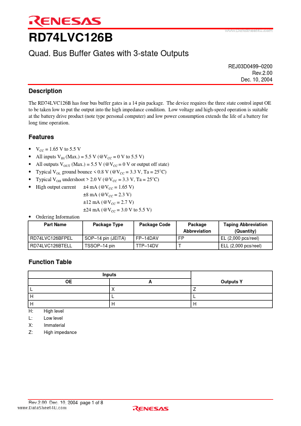
 Features VCC = 1.65 V to 5.5 V All inputs VIH (Max.) = 5.5 V (@VCC = 0 V to 5.5 V) All outputs VOUT (Max.) = 5.5 V (@VCC = 0 V or output off state) Typical VOL ground bounce < 0.8 V (@VCC = 3.3 V, Ta = 25°C) Typical VOH undershoot > 2.0 V (@VCC = 3.