RD74LVC1G125
RD74LVC1G125 is Bus Buffer manufactured by Renesas.
..
Bus Buffer with 3- state Output
REJ03D0731- 0100 Rev.1.00 Apr 13, 2006
Description
The RD74LVC1G125 has bus buffer with 3- state output in a 5-pin package. Low voltage and high-speed operation is suitable for the battery powered products (e.g., notebook puters), and the low power consumption extends the battery life.
Features
The basic gate function is lined up as renesas uni logic series. Supply voltage range: 1.65 to 5.5 V Operating temperature range:
- 40 to +85°C All inputs: VIH (Max.) = 5.5 V (@VCC = 0 V to 5.5 V) All outputs: VO (Max.) = 5.5 V (@VCC = 0 V) Output current: ±4 m A (@VCC = 1.65 V) ±8 m A (@VCC = 2.3 V) ±24 m A (@VCC = 3.0 V) ±32 m A (@VCC = 4.5 V)
- Ordering Information
Part Name RD74LVC1G125WPE Package Type WCSP- 5 pin Package Code (Previous Code) SXBG0005LB- A (TBS- 5CV) Package Abbreviation WP Taping Abbreviation (Quantity) E (3,000 pcs/reel)
- -
- -
- -
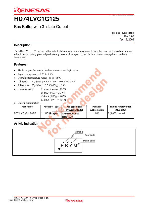
Article Indication
Marking Year code Month code
EBYM
Rev.1.00 Apr 13, 2006 page 1 of 7
Function Table
Inputs OE L L H H: High level L: Low level X: Immaterial Z: High impedance A H L X
..
Output Y H L Z
Pin Arrangement
0.7 mm Height 0.4 mm 0.4 mm pitch 0.17 mm 5- Ball (WP) GND
1.1 mm
Pin#1 INDEX
(Bottom view)
(Top view)
Logic Diagram
O OE A 1 2 4 Y
Rev.1.00 Apr 13, 2006 page 2 of...