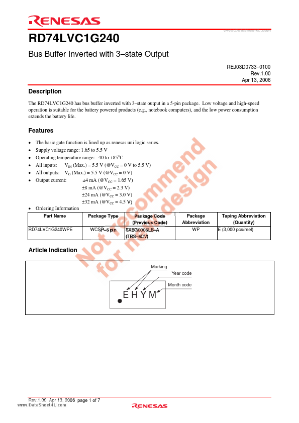
Datasheet4U Logo Datasheet4U.com

RD74LVC1G240 - Bus Buffer Inverted

Description

The RD74LVC1G240 has bus buffer inverted with 3

state output in a 5-pin package.

Low voltage and high-speed operation is suitable for the battery powered products (e.g., notebook computers), and the low power consumption extends the battery life.

Features

  • The basic gate function is lined up as renesas uni logic series. Supply voltage range: 1.65 to 5.5 V Operating temperature range:.
  • 40 to +85°C All inputs: VIH (Max. ) = 5.5 V (@VCC = 0 V to 5.5 V) All outputs: VO (Max. ) = 5.5 V (@VCC = 0 V) Output current: ±4 mA (@VCC = 1.65 V) ±8 mA (@VCC = 2.3 V) ±24 mA (@VCC = 3.0 V) ±32 mA (@VCC = 4.5 V).
  • Ordering Information Part Name RD74LVC1G240WPE Package Type WCSP.
  • 5 pin.

📥 Download Datasheet

Other Datasheets by Renesas Technology

Full PDF Text Transcription

Click to expand full text
www.DataSheet4U.com RD74LVC1G240 Bus Buffer Inverted with 3–state Output REJ03D0733–0100 Rev.1.00 Apr 13, 2006 Description The RD74LVC1G240 has bus buffer inverted with 3–state output in a 5-pin package. Low voltage and high-speed operation is suitable for the battery powered products (e.g., notebook computers), and the low power consumption extends the battery life. Features • • • • • • The basic gate function is lined up as renesas uni logic series. Supply voltage range: 1.65 to 5.5 V Operating temperature range: –40 to +85°C All inputs: VIH (Max.) = 5.5 V (@VCC = 0 V to 5.5 V) All outputs: VO (Max.) = 5.5 V (@VCC = 0 V) Output current: ±4 mA (@VCC = 1.65 V) ±8 mA (@VCC = 2.3 V) ±24 mA (@VCC = 3.0 V) ±32 mA (@VCC = 4.
Published: |