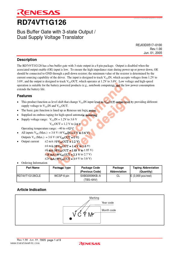
Datasheet4U Logo Datasheet4U.com

RD74VT1G126 - Bus Buffer Gate with 3-state output / Dual Supply Voltage Translator

Datasheet Summary

Description

The RD74VT1G126 has a bus buffer gate with 3-state output in a 6 pin package.

Output is disabled when the associated output enable (OE) input is low.

Features

  • This product function as level shift that change VCCIN input level to VCCOUT output level by providing different supply voltage to VCCIN and VCCOUT.
  • The basic gate function is lined up as Renesas uni logic series.
  • Supplied on emboss taping for high-speed automatic mounting.
  • Supply voltage range: VCCIN = 1.2V to 3.6 V VCCOUT = 1.2 V to 3.6 V Operating temperature range:.
  • 40 to +85°C.
  • All inputs VIH (Max. ) = 3.6 V (@VCCIN = 0 V to 3.6 V) Out.

📥 Download Datasheet

Datasheet preview – RD74VT1G126

Datasheet Details

Part number RD74VT1G126
Manufacturer Renesas Technology
File Size 2.46 MB
Description Bus Buffer Gate with 3-state output / Dual Supply Voltage Translator
Datasheet download datasheet RD74VT1G126 Datasheet
Additional preview pages of the RD74VT1G126 datasheet.
Other Datasheets by Renesas Technology

Full PDF Text Transcription

Click to expand full text
www.DataSheet4U.com RD74VT1G126 Bus Buffer Gate with 3-state Output / Dual Supply Voltage Translator REJ03D0517–0100 Rev.1.00 Jun. 01, 2005 Description The RD74VT1G126 has a bus buffer gate with 3-state output in a 6 pin package. Output is disabled when the associated output enable (OE) input is low. To ensure the high impedance state during power up or power down, OE should be connected to GND through a pull-down resistor; the minimum value of the resistor is determined by the current sourcing capability of the driver. The input is designed to track VCCIN, which accepts voltages from 1.2V to 3.6V, and the output is designed to track VCCOUT, which operates at 1.2V to 3.6V. Low voltage and high-speed operation is suitable for the battery powered products (e.g.
Published: |