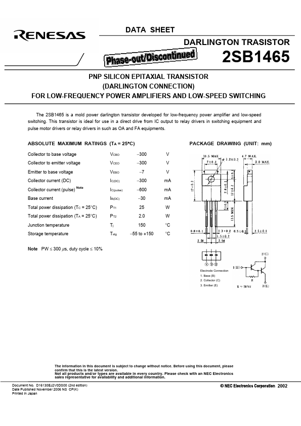
ABSOLUTE MAXIMUM RATINGS
(TA = 25°C) Collector to base voltage Collector to emitter voltage Emitter to base voltage Collector current (DC) Collector current (pulse) Note Base current Total power dissipation (TC = 25°C) Total power dissipation (TA = 25°C) Junction temperature Storage temperature VCBO VCEO VEBO IC(DC) IC(pulse) IB(DC) PT1 PT2 Tj Tstg −300 −300 −7 −300 −600 −30 25 2.0 150 −55 to +150 V V V mA mA mA W W °C °C PACKAGE DRAWING (UNIT: mm) Note PW ≤ 300 μs, duty cycle ≤ 10% Electrode Connection 1. Base (B) 2. Collector (C) 3. Emitter (E) The information in this document is subject to change without notice. Before using this document, please confirm that this is the latest version. Not all products and/or types are available in every country. Please check with an NEC Electronics sales representative for availability and additional information. Document No. D16130EJ2V0DS00 (2nd edition) Date Published November 2006 NS CP(K) Printed in Japan 2002 2SB1465 ELECTRICAL CHARACTERISTIC... Renesas Electronics