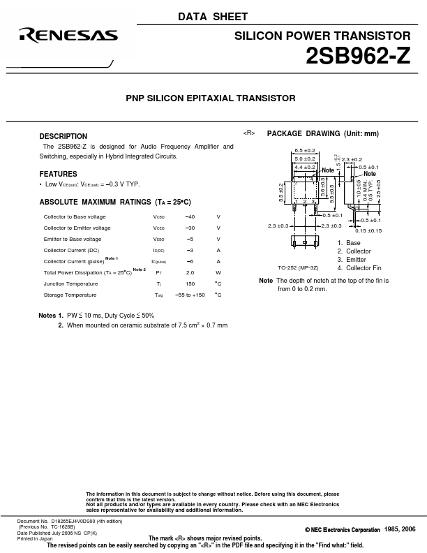
DESCRIPTION
<R> FEATURES
● Low VCE(sat): VCE(sat) = −0.3 V TYP. PACKAGE DRAWING (Unit: mm) 6.5 ±0.2 5.0 ±0.2 4.4 ±0.2 4 Note 1.5 +0.2 −0.1 2.3 ±0.2 0.5 ±0.1 Note 1.0 ±0.5 0.4 MIN. 0.5 TYP. 2.5 ±0.5 5.6 ±0.3 9.5 ±0.5 5.5 ±0.2 ABSOLUTE MAXIMUM RATINGS
(TA = 25°C) Collector to Base voltage VCBO −40 V Collector to Emitter voltage VCEO −30 V Emitter to Base voltage VEBO −5 V Collector Current (DC) IC(DC) −3 A Collector Current (pulse) Note 1 IC(pulse) −6 A Total Power Dissipation (TA = 25°C) Note 2 PT 2.0 W Junction Temperature Tj 150 °C Storage Temperature Tstg −55 to +150 °C 123 2.3 ±0.3 0.5 ±0.1 2.3 ±0.3 0.5 ±0.1 0.15 ±0.15 TO-252 (MP-3Z) 1. Base 2. Collector 3. Emitter 4. Collector Fin Note The depth of notch at the top of the fin is from 0 to 0.2 mm. Notes 1. PW ≤ 10 ms, Duty Cycle ≤ 50% 2. When mounted on ceramic substrate of 7.5 cm2 × 0.7 mm The information in this document is subject to change without notice. Before using this document, please confirm that this is the latest version. Renesas Electronics