524S
Description
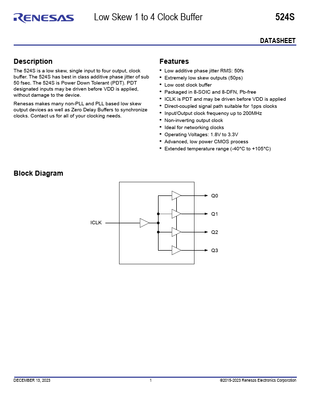
The 524S is a low skew, single input to four output, clock buffer.
Key Features
- Low additive phase jitter RMS: 50fs
- Extremely low skew outputs (50ps)
- Low cost clock buffer
- Packaged in 8-SOIC and 8-DFN, Pb-free
- ICLK is PDT and may be driven before VDD is applied
- Direct-coupled signal path suitable for 1pps clocks
- Input/Output clock frequency up to 200MHz
- Non-inverting output clock
- Ideal for networking clocks
- Operating Voltages: 1.8V to 3.3V