553S
553S is Low Skew 1 to 4 Clock Buffer manufactured by Renesas.
Low Skew 1 to 4 Clock Buffer
553S Datasheet
Description
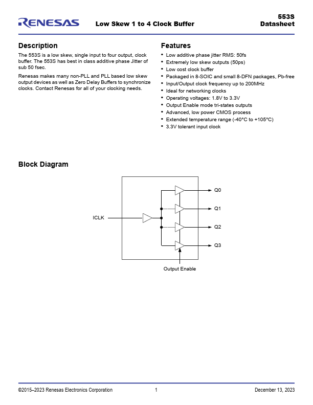
The 553S is a low skew, single input to four output, clock buffer. The 553S has best in class additive phase Jitter of sub 50 fsec.
Renesas makes many non-PLL and PLL based low skew output devices as well as Zero Delay Buffers to synchronize clocks. Contact Renesas for all of your clocking needs.
Features
- Low additive phase jitter RMS: 50fs
- Extremely low skew outputs (50ps)
- Low cost clock buffer
- Packaged in 8-SOIC and small 8-DFN packages, Pb-free
- Input/Output clock frequency up to 200MHz
- Ideal for networking clocks
- Operating voltages: 1.8V to 3.3V
- Output Enable mode tri-states outputs
- Advanced, low power CMOS process
- Extended temperature range (-40°C to +105°C)
- 3.3V tolerant input clock
Block Diagram
ICLK
Q0 Q1 Q2 Q3
Output Enable
©2015- 2023 Renesas Electronics Corporation
December 13, 2023
Pin Assignments
Q0
Q1
Q3
Q2
ICLK
8-pin...