Renesas Electronics 557G06LF
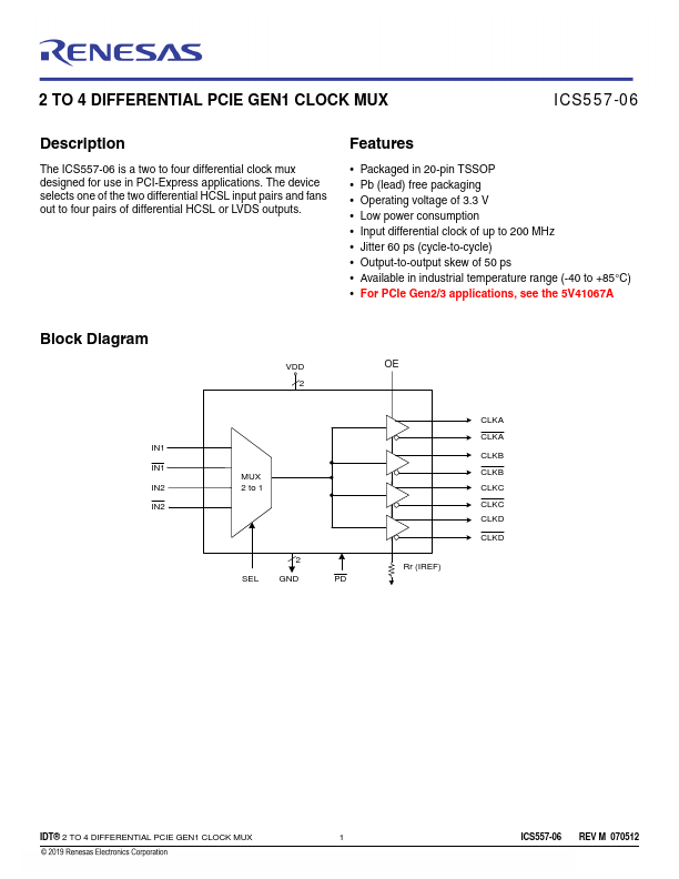
The ICS557-06 is a two to four differential clock mux designed for use in PCI-Express applications. The device selects one of the two differential HCSL input pairs and fans out to four pairs of differential HCSL or LVDS outputs.| Part No. | 557G06LF |
|---|---|
| Datasheet | 557G06LF Download |
| Manufacturer |  Renesas Electronics |
| Description | 2 TO 4 DIFFERENTIAL PCIE GEN1 CLOCK MUX |
| Buy | Stock & Price |
DESCRIPTION
FEATURES
● Packaged in 20-pin TSSOP● Pb (lead) free packaging
● Operating voltage of 3.3 V
● Low power consumption
● Input differential clock of up to 200 MHz
● Jitter 60 ps (cycle-to-cycle)
● Output-to-output skew of 50 ps
● Available in industrial temperature range (-40 to +85°C)
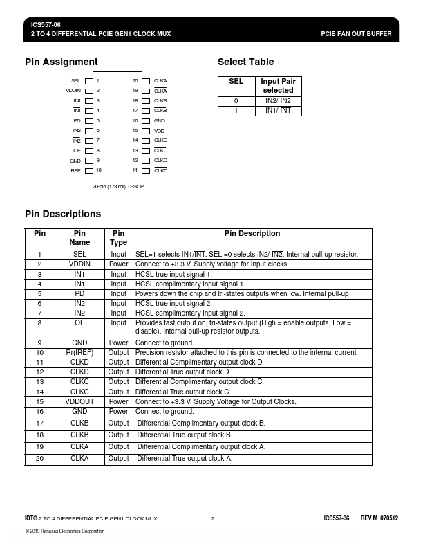
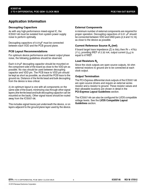
● For PCIe Gen2/3 applications, see the 5V41067A Block Diagram IN1 IN1 IN2 IN2 VDD 2 MUX 2 to 1 2 SEL GND PD OE Rr (IREF) CLKA CLKA CLKB CLKB CLKC CLKC CLKD CLKD IDT® 2 TO 4 DIFFERENTIAL PCIE GEN1 CLOCK MUX 1 ICS557-06 REV M 070512 ICS557-06 2 TO 4 DIFFERENTIAL PCIE GEN1 CLOCK MUX PCIE FAN OUT BUFFER Pin Assignment SEL 1 VDDIN 2 IN1 3 IN1 4 PD 5 IN2 6 IN2 7 OE 8 GND 9 IREF 10 20 CLKA 19 CLKA 18 CLKB 17 CLKB 16 GND 15 VDD 14 CLKC 13 CLKC 12 CLKD 11 CLKD 20-pin (173 mil) TSSOP Select Table SEL 0 1 Input Pair selected IN2/ IN2 IN1/ IN1 Pin Descriptions Pin Pin Pin Name Type Pin
DESCRIPTION
1 SEL Input SEL=1 selects IN1/IN1. SEL =0 selects IN2/ IN2. Internal pull-up resistor. 2 VDDIN Power Connect to +3.3 V.