557GI06LF
557GI06LF is 2 TO 4 DIFFERENTIAL PCIE GEN1 CLOCK MUX manufactured by Renesas.
- Part of the 557G06LF comparator family.
- Part of the 557G06LF comparator family.
2 TO 4 DIFFERENTIAL PCIE GEN1 CLOCK MUX
ICS557-06
Description
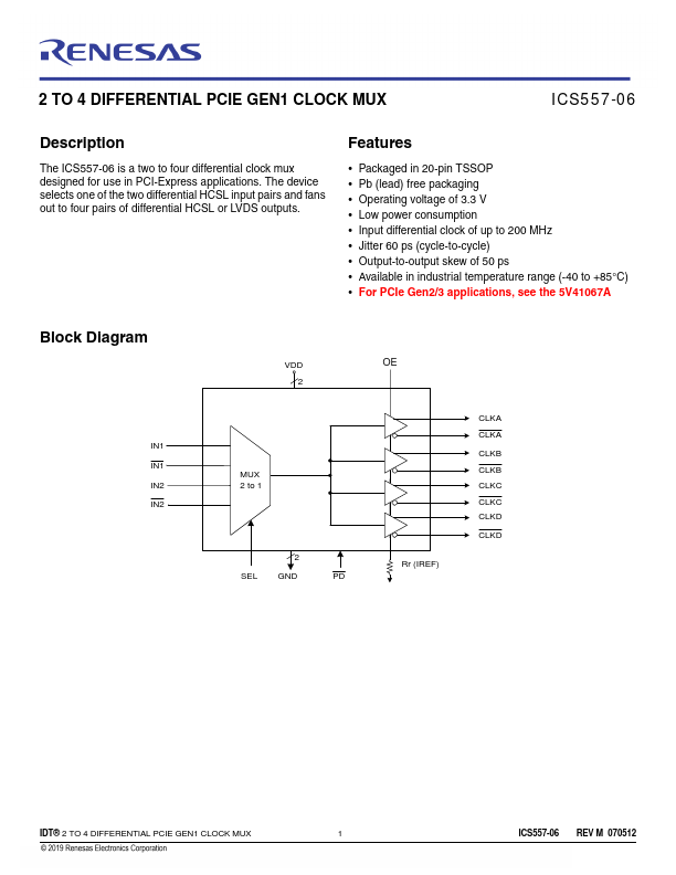
The ICS557-06 is a two to four differential clock mux designed for use in PCI-Express applications. The device selects one of the two differential HCSL input pairs and fans out to four pairs of differential HCSL or LVDS outputs.
Features
- Packaged in 20-pin TSSOP
- Pb (lead) free packaging
- Operating voltage of 3.3 V
- Low power consumption
- Input differential clock of up to 200 MHz
- Jitter 60 ps (cycle-to-cycle)
- Output-to-output skew of 50 ps
- Available in industrial temperature range (-40 to +85°C)
- For PCIe Gen2/3 applications, see the 5V41067A
Block Diagram
IN1 IN1 IN2 IN2
VDD 2
MUX 2 to 1
SEL GND
Rr (IREF)
CLKA CLKA CLKB CLKB CLKC CLKC CLKD CLKD
IDT® 2 TO 4 DIFFERENTIAL PCIE GEN1 CLOCK MUX
ICS557-06 REV M 070512
ICS557-06 2 TO 4 DIFFERENTIAL PCIE GEN1 CLOCK MUX
PCIE FAN OUT BUFFER
Pin Assignment
VDDIN
IN1
IN1
IN2...