Renesas Electronics 5P1105
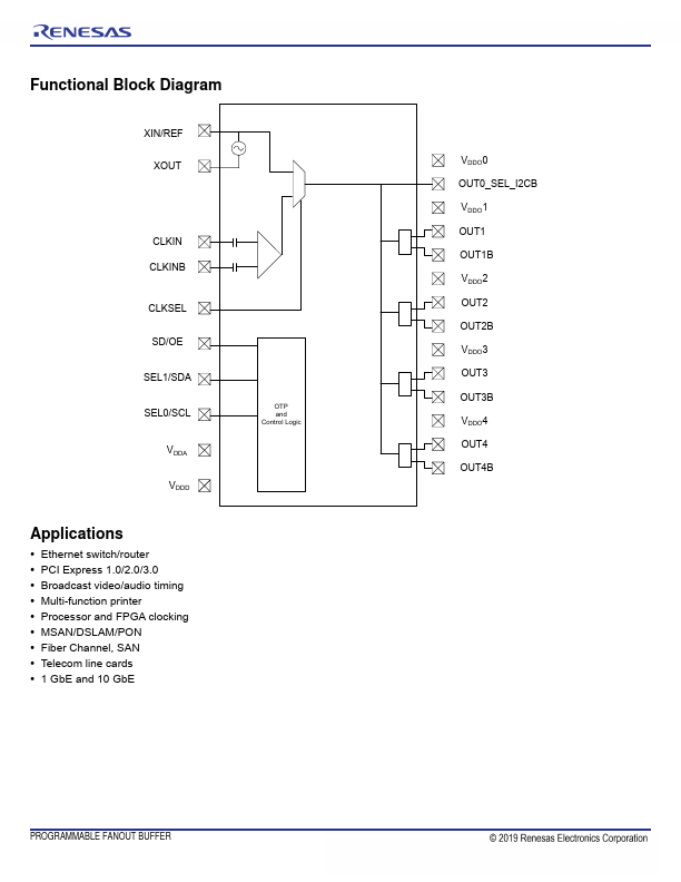
The 5P1105 is a programmable fanout buffer intended for high performance consumer, networking, industrial, computing, and data-communications applications. The outputs are generated from a single reference clock. The reference clock can come from one of the two redundant clock inputs.| Part No. | 5P1105 |
|---|---|
| Datasheet | 5P1105 Download |
| Manufacturer |  Renesas Electronics |
| Description | Programmable Fanout Buffer |
| Buy | Stock & Price |
DESCRIPTION
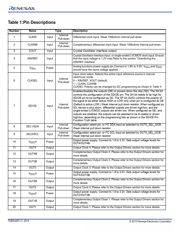
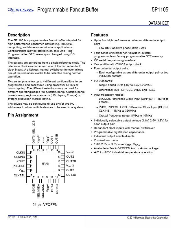
Configurations may be stored in on-chip One-Time Programmable (OTP) memory or changed using I2C interface. A glitchless manual switchover function allows one of the redundant clocks to be selected during normal operation. Two select pins allow up to 4 different configurations to be programmed and accessible using processor GPIOs or bootstrapping. The different selections may be used for different operating modes (full function, partial function, partial power-down), regional standards (US, Japan, Europe) or system production margin testing. The device may be configured to use one of two I2C addresses to allow multiple devices to be used in a system. Pin Assignment OUT0_SEL_I2CB VDDO0 VDDD VDDO1 OUT1 OUT1B CLKIN CLKINB XOUT XIN/REF VDDA CLKSEL 1 24 23 22 21 20 19 18 2 17 3 16 EPAD 4 15 5 14 6 13 7 8 9 10 11 12 VDDO2 OUT2 OUT2B VDDO3 OUT3 OUT3BFEATURES
● Up to four high performance universal differential output pairs – Low RMS additive phase jitter: 0.2ps● Four banks of int...