5P49V5908
5P49V5908 is Programmable Clock Generator manufactured by Renesas.
Description
The 5P49V5908 is a programmable clock generator intended for high performance consumer, networking, industrial, puting, and data-munications applications. Configurations may be stored in on-chip One-Time Programmable (OTP) memory or changed using I2C interface. This is IDTs fifth generation of programmable clock technology (Versa Clock® 5).
The frequencies are generated from a single reference clock or crystal. Two select pins allow up to 4 different configurations to be programmed and accessible using processor GPIOs or bootstrapping. The different selections may be used for different operating modes (full function, partial function, partial power-down), regional standards (US, Japan, Europe) or system production margin testing.
The device may be configured to use one of two I2C addresses to allow multiple devices to be used in a system.
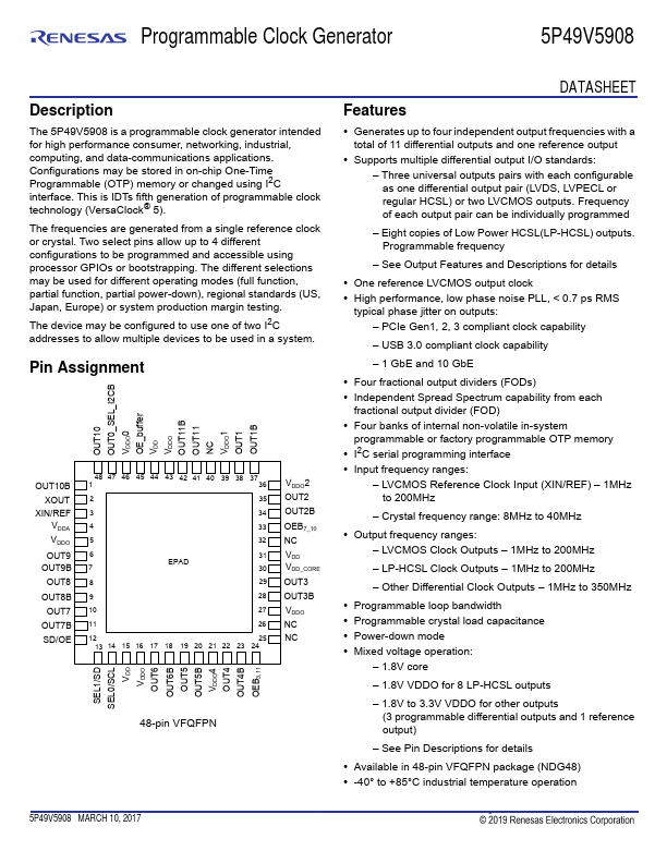
Pin Assignment
OUT10 OUT0_SEL_I2CB VDDO0 OE_buffer VDD VDDO OUT11B OUT11 NC VDDO1 OUT1 OUT1B
OUT10B XOUT
XIN/REF VDDA VDDO
OUT9 OUT9B
OUT8
OUT8B OUT7
OUT7B SD/OE
48 47 46 45 44 43 42 41 40 39 38 37 1 36 2 35 3 34 4 33 5 32 6 31
EPAD 7 30 8 29 9 28 10 27 11 26 12 25
13 14 15 16 17 18 19 20 21 22 23 24
VDDO2 OUT2 OUT2B
OEB7_10 NC VDD VDD_CORE OUT3 OUT3B VDDO NC NC
SEL1/SD SEL0/SCL
VDD VDDO OUT6 OUT6B OUT5 OUT5B VDDO4 OUT4 OUT4B OEB3,11
48-pin VFQFPN
Features
- Generates up to four independent output frequencies with a total of 11 differential outputs and one reference output
- Supports multiple differential output I/O standards:
- Three universal outputs pairs with each configurable as one differential output pair (LVDS, LVPECL or regular HCSL) or two LVCMOS outputs. Frequency of each output pair can be individually programmed
- Eight copies of Low Power HCSL(LP-HCSL) outputs. Programmable frequency
- See Output Features and Descriptions for details
- One reference LVCMOS output clock
- High performance, low phase noise PLL, < 0.7 ps RMS typical phase jitter on outputs:
- PCIe Gen1, 2, 3 pliant clock...