5P49V5933
Description
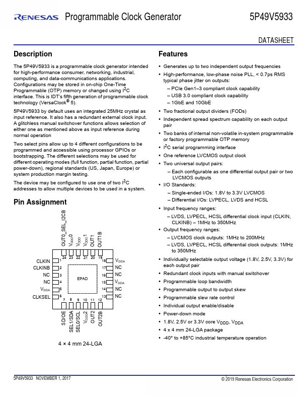
The 5P49V5933 is a programmable clock generator intended for high-performance consumer, networking, industrial, puting, and data-munications applications.
Key Features
- Generates up to two independent output frequencies
- High-performance, low-phase noise PLL, < 0.7ps RMS
- Two fractional output dividers (FODs)
- Independent spread spectrum capability on each output
- Two banks of internal non-volatile in-system programmable
- I2C serial programming interface
- One reference LVCMOS output clock
- Two universal output pairs
- I/O Standards
- Input frequency ranges
Applications
- Ethernet switch/router