5P49V6968
5P49V6968 is Clock Generator manufactured by Renesas.
Description
The 5P49V6968 is a programmable clock generator that is intended for high-performance consumer, networking, industrial, puting, and data munications applications. This is Renesas’ sixth generation of programmable clock technology (Versa Clock 6E).
The 5P49V6968 generates the frequencies from a single reference clock, which can originate from one of the two redundant clock inputs. A glitchless manual switchover function allows one of the redundant clocks to be selected during normal operation.
Two select pins allow up to four different configurations to be programmed and can be used for different operating modes.
Typical Applications
- Ethernet switch/router
- PCI Express 1.0/2.0/3.0/4.0 spread spectrum on
- PCI Express 1.0/2.0/3.0/4.0/5.0 spread spectrum off
- Broadcast video/audio timing
- Multi-function printer
- Processor and FPGA clocking
- Any-frequency clock conversion
- MSAN/DSLAM/PON
- Fiber Channel, SAN
- Tele line cards
- Datacenter
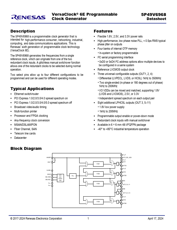
Block Diagram
XIN/REF XOUT
CLKSEL
SD/OE
SEL1/SDA and
SEL0/SCL
Control Logic
VDDA VDDD
Features
- Flexible 1.8V, 2.5V, and 3.3V power rails
- High-performance, low phase noise PLL, < 0.5ps RMS typical phase jitter on outputs
- Four banks of internal OTP memory
- In-system or factory programmable
- I2C serial programming interface
- 0x D0 or 0x D4 I2C address options allow multiple devices to be configured in a same system
- Reference LVCMOS output clock
- Three universal configurable outputs (OUT1, 2, 4):
- Differential (LVPECL, LVDS, or HCSL) 1k Hz to 350MHz
- Two single-ended (in-phase or 180 degrees out of phase) 1k Hz to 200MHz
- I/O VDDs can be mixed and matched, supporting 1.8V (LVDS and LVCMOS), 2.5V, or 3.3V
- Independent spread spectrum on each output pair
- Eight additional LPHCSL outputs (OUT 3, 5-...