Datasheet4U Logo Datasheet4U.com

5PB1102PGG - 1.8V to 3.3V High-Performance LVCMOS Clock Buffer

General Description

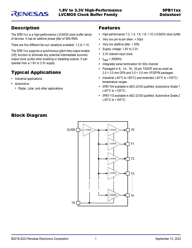
The 5PB11xx is a high-performance LVCMOS clock buffer family of devices.

It has an additive phase jitter of 50fs RMS.

There are five different fan-out variations available: 1:2 to 1:10.

Key Features

  • High-performance 1:2, 1:4, 1:6, 1:8, 1:10 LVCMOS clock buffer.
  • Very low pin-to-pin skew: < 50ps.
  • Very low additive jitter: < 50fs.
  • Supply voltage: 1.8V to 3.3V.
  • 3.3V tolerant input clock.
  • fMAX = 200MHz.
  • Integrated serial termination for 50Ω channel.
  • Packaged in 8-, 14-, 16-, 20-pin TSSOP and as small as 2.0 × 2.0 mm DFN and 3.0 × 3.0 mm VFQFPN packages.
  • Industrial (-40°C to +85°C) and extended (-40°C to +105°C) temperature ranges.
  • 5PB1104 availa.

📥 Download Datasheet

Datasheet Details

Part number 5PB1102PGG
Manufacturer Renesas
File Size 1.99 MB
Description 1.8V to 3.3V High-Performance LVCMOS Clock Buffer
Datasheet download datasheet 5PB1102PGG Datasheet

Full PDF Text Transcription (Reference)

The following content is an automatically extracted verbatim text from the original manufacturer datasheet and is provided for reference purposes only.

View original datasheet text
1.8V to 3.3V High-Performance LVCMOS Clock Buffer Family 5PB11xx Datasheet Description The 5PB11xx is a high-performance LVCMOS clock buffer family of devices. It has an additive phase jitter of 50fs RMS. There are five different fan-out variations available: 1:2 to 1:10. The 5PB11xx supports a synchronous glitch-free output enable (OE) function to eliminate any potential intermediate incorrect output clock cycles when enabling or disabling outputs. It can operate from a 1.8V to 3.3V supply. Typical Applications ▪ Industrial applications ▪ Automotive: • Radar, Lidar, and other applications Features ▪ High-performance 1:2, 1:4, 1:6, 1:8, 1:10 LVCMOS clock buffer ▪ Very low pin-to-pin skew: < 50ps ▪ Very low additive jitter: < 50fs ▪ Supply voltage: 1.8V to 3.3V ▪ 3.